- Joined
- Oct 9, 2007
- Messages
- 47,774 (7.41/day)
- Location
- Dublin, Ireland
| System Name | RBMK-1000 |
|---|---|
| Processor | AMD Ryzen 7 5700G |
| Motherboard | Gigabyte B550 AORUS Elite V2 |
| Cooling | DeepCool Gammax L240 V2 |
| Memory | 2x 16GB DDR4-3200 |
| Video Card(s) | Galax RTX 4070 Ti EX |
| Storage | Samsung 990 1TB |
| Display(s) | BenQ 1440p 60 Hz 27-inch |
| Case | Corsair Carbide 100R |
| Audio Device(s) | ASUS SupremeFX S1220A |
| Power Supply | Cooler Master MWE Gold 650W |
| Mouse | ASUS ROG Strix Impact |
| Keyboard | Gamdias Hermes E2 |
| Software | Windows 11 Pro |
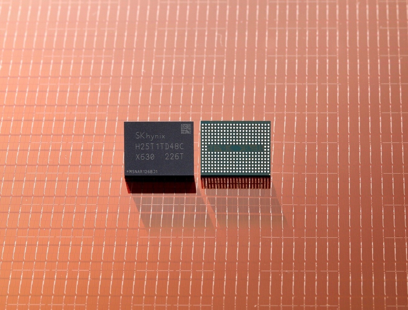
SK hynix Inc. announced today that it has developed the industry's highest 238-layer NAND Flash product. The company has recently shipped samples of the 238-layer 512Gb triple level cell (TLC) 4D NAND product to customers with a plan to start mass production in the first half of 2023. "The latest achievement follows development of the 176-layer NAND product in December 2020," the company stated. "It is notable that the latest 238-layer product is most layered and smallest in area at the same time."
The company unveiled development of the latest product at the Flash Memory Summit 2022 in Santa Clara. "SK hynix secured global top-tier competitiveness in perspective of cost, performance and quality by introducing the 238-layer product based on its 4D NAND technologies," said Jungdal Choi, Head of NAND Development at SK hynix in his keynote speech during the event. "We will continue innovations to find breakthroughs in technological challenges."

Since development of the 96-layer NAND product in 2018, SK hynix has introduced a series of 4D products that outperform existing 3D products. The company has applied charge trap flash and peri under cell technologies to make chips with 4D structures. 4D products have a smaller cell area per unit compared with 3D, leading to higher production efficiency.
The product, while achieving highest layers of 238, is the smallest NAND in size, meaning its overall productivity has increased by 34% compared with the 176-layer NAND, as more chips with higher density per unit area can be produced from each wafer.
The data-transfer speed of the 238-layer product is 2.4Gb per second, a 50% increase from the previous generation. The volume of the energy consumed for data reading has decreased by 21%, an achievement that also meets the company's ESG commitment.
The 238-layer products will be first adopted for client SSDs which are used as PC storage devices, before being provided for smartphones and high-capacity SSDs for servers later. The company will also introduce 238-layer products in 1 Terabit (Tb) next year, with density doubled compared to the current 512Gb product.
View at TechPowerUp Main Site
The company unveiled development of the latest product at the Flash Memory Summit 2022 in Santa Clara. "SK hynix secured global top-tier competitiveness in perspective of cost, performance and quality by introducing the 238-layer product based on its 4D NAND technologies," said Jungdal Choi, Head of NAND Development at SK hynix in his keynote speech during the event. "We will continue innovations to find breakthroughs in technological challenges."
Since development of the 96-layer NAND product in 2018, SK hynix has introduced a series of 4D products that outperform existing 3D products. The company has applied charge trap flash and peri under cell technologies to make chips with 4D structures. 4D products have a smaller cell area per unit compared with 3D, leading to higher production efficiency.
The product, while achieving highest layers of 238, is the smallest NAND in size, meaning its overall productivity has increased by 34% compared with the 176-layer NAND, as more chips with higher density per unit area can be produced from each wafer.
The data-transfer speed of the 238-layer product is 2.4Gb per second, a 50% increase from the previous generation. The volume of the energy consumed for data reading has decreased by 21%, an achievement that also meets the company's ESG commitment.
The 238-layer products will be first adopted for client SSDs which are used as PC storage devices, before being provided for smartphones and high-capacity SSDs for servers later. The company will also introduce 238-layer products in 1 Terabit (Tb) next year, with density doubled compared to the current 512Gb product.
View at TechPowerUp Main Site


")

