TheLostSwede
News Editor
- Joined
- Nov 11, 2004
- Messages
- 18,967 (2.51/day)
- Location
- Sweden
| System Name | Overlord Mk MLI |
|---|---|
| Processor | AMD Ryzen 7 7800X3D |
| Motherboard | Gigabyte X670E Aorus Master |
| Cooling | Noctua NH-D15 SE with offsets |
| Memory | 32GB Team T-Create Expert DDR5 6000 MHz @ CL30-34-34-68 |
| Video Card(s) | Gainward GeForce RTX 4080 Phantom GS |
| Storage | 1TB Solidigm P44 Pro, 2 TB Corsair MP600 Pro, 2TB Kingston KC3000 |
| Display(s) | Acer XV272K LVbmiipruzx 4K@160Hz |
| Case | Fractal Design Torrent Compact |
| Audio Device(s) | Corsair Virtuoso SE |
| Power Supply | be quiet! Pure Power 12 M 850 W |
| Mouse | Logitech G502 Lightspeed |
| Keyboard | Corsair K70 Max |
| Software | Windows 10 Pro |
| Benchmark Scores | https://valid.x86.fr/yfsd9w |
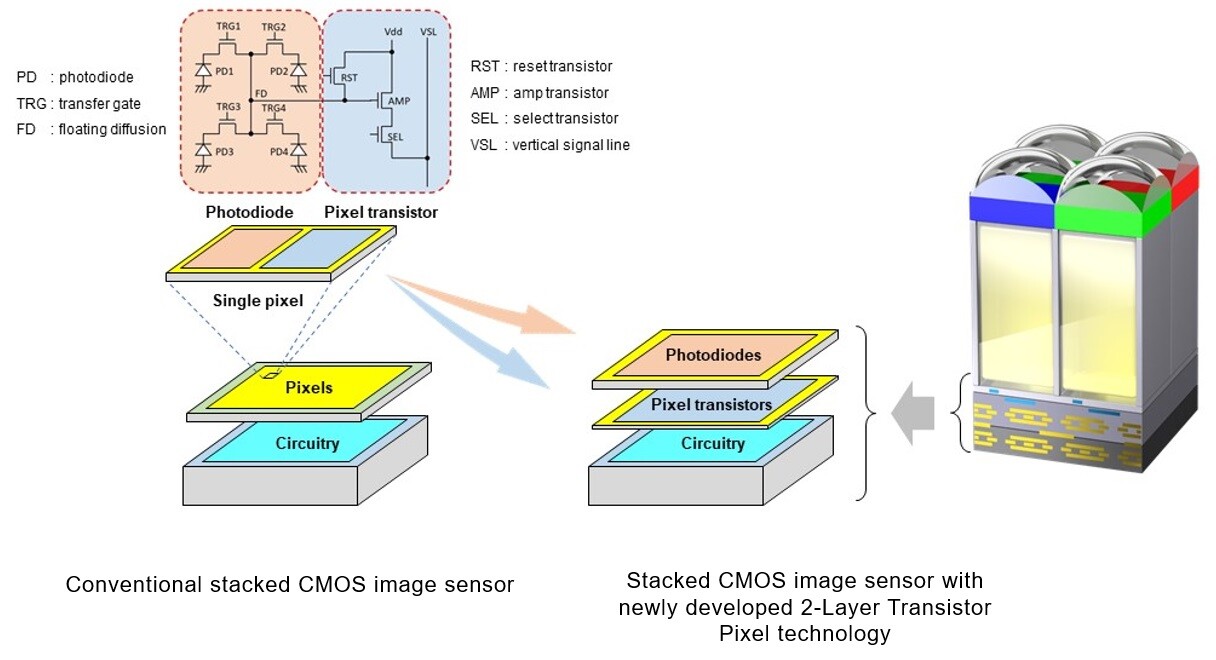
Sony Semiconductor Solutions Corporation has succeeded in developing the world's first stacked CMOS image sensor technology with 2-Layer Transistor Pixel. Whereas conventional CMOS image sensors' photodiodes and pixel transistors occupy the same substrate, Sony's new technology separates photodiodes and pixel transistors on different substrate layers. This new architecture approximately doubles saturation signal level relative to conventional image sensors, widens dynamic range and reduces noise, thereby substantially improving imaging properties. The new technology's pixel structure will enable pixels to maintain or improve their existing properties at not only current but also smaller pixel sizes.
A stacked CMOS image sensor adopts a stacked structure consisting of a pixel chip made up of back-illuminated pixels stacked atop a logic chip where signal processing circuits are formed. Within the pixel chip, photodiodes for converting light to electrical signals, and pixel transistors for controlling the signals are situated alongside each other on the same layer. Increasing saturation signal level within form-factor constraints plays an important role in realizing high image quality with wide dynamic range.

Sony's new architecture is an advancement in stacked CMOS image sensor technology. Using its proprietary stacking technology, Sony packaged the photodiodes and pixel transistors on separate substrates stacked one atop the other.
In conventional stacked CMOS image sensors, by contrast, the photodiodes and pixel transistors sit alongside each other on the same substrate. The new stacking technology enables adoption of architectures that allow the photodiode and pixel transistor layers to each be optimized, thereby approximately doubling saturation signal level relative to conventional image sensors and, in turn, widening dynamic range.
Additionally, because pixel transistors other than transfer gates (TRG), including reset transistors (RST), select transistors (SEL) and amp transistors (AMP), occupy a photodiode-free layer, the amp transistors can be increased in size. By increasing amp transistor size, Sony succeeded in substantially reducing the noise to which nighttime and other dark-location images are prone.
The widened dynamic range and noise reduction available from this new technology will prevent underexposure and overexposure in settings with a combination of bright and dim illumination (e.g., backlit settings) and enable high-quality, low-noise images even in low-light (e.g., indoor, nighttime) settings.
Sony will contribute to the realization of increasingly high-quality imaging such as smartphone photographs with its 2-Layer Transistor Pixel technology.
View at TechPowerUp Main Site
A stacked CMOS image sensor adopts a stacked structure consisting of a pixel chip made up of back-illuminated pixels stacked atop a logic chip where signal processing circuits are formed. Within the pixel chip, photodiodes for converting light to electrical signals, and pixel transistors for controlling the signals are situated alongside each other on the same layer. Increasing saturation signal level within form-factor constraints plays an important role in realizing high image quality with wide dynamic range.
Sony's new architecture is an advancement in stacked CMOS image sensor technology. Using its proprietary stacking technology, Sony packaged the photodiodes and pixel transistors on separate substrates stacked one atop the other.
In conventional stacked CMOS image sensors, by contrast, the photodiodes and pixel transistors sit alongside each other on the same substrate. The new stacking technology enables adoption of architectures that allow the photodiode and pixel transistor layers to each be optimized, thereby approximately doubling saturation signal level relative to conventional image sensors and, in turn, widening dynamic range.
Additionally, because pixel transistors other than transfer gates (TRG), including reset transistors (RST), select transistors (SEL) and amp transistors (AMP), occupy a photodiode-free layer, the amp transistors can be increased in size. By increasing amp transistor size, Sony succeeded in substantially reducing the noise to which nighttime and other dark-location images are prone.
The widened dynamic range and noise reduction available from this new technology will prevent underexposure and overexposure in settings with a combination of bright and dim illumination (e.g., backlit settings) and enable high-quality, low-noise images even in low-light (e.g., indoor, nighttime) settings.
Sony will contribute to the realization of increasingly high-quality imaging such as smartphone photographs with its 2-Layer Transistor Pixel technology.
View at TechPowerUp Main Site
