T0@st
News Editor
- Joined
- Mar 7, 2023
- Messages
- 3,063 (3.89/day)
- Location
- South East, UK
| System Name | The TPU Typewriter |
|---|---|
| Processor | AMD Ryzen 5 5600 (non-X) |
| Motherboard | GIGABYTE B550M DS3H Micro ATX |
| Cooling | DeepCool AS500 |
| Memory | Kingston Fury Renegade RGB 32 GB (2 x 16 GB) DDR4-3600 CL16 |
| Video Card(s) | PowerColor Radeon RX 7800 XT 16 GB Hellhound OC |
| Storage | Samsung 980 Pro 1 TB M.2-2280 PCIe 4.0 X4 NVME SSD |
| Display(s) | Lenovo Legion Y27q-20 27" QHD IPS monitor |
| Case | GameMax Spark M-ATX (re-badged Jonsbo D30) |
| Audio Device(s) | FiiO K7 Desktop DAC/Amp + Philips Fidelio X3 headphones, or ARTTI T10 Planar IEMs |
| Power Supply | ADATA XPG CORE Reactor 650 W 80+ Gold ATX |
| Mouse | Roccat Kone Pro Air |
| Keyboard | Cooler Master MasterKeys Pro L |
| Software | Windows 10 64-bit Home Edition |
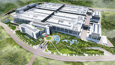
Earlier in the year, we heard about TSMC being ahead of the game with its speculated trial production run of cutting-edge 2 nm (N2) silicon. Taiwan's premier foundry company is reportedly prepping its Baoshan and Kaohsiung plants for full-on manufacturing of next-gen chips. The latest insider whispers propose that TSMC is making "rapid" progress on the 2 nm (N2) front, as company engineers have moved onto an "intensive" trial production phase. Taiwan's Economic Daily News has picked up on compelling projections from industry moles; the Hsinchu Baoshan facility's current monthly production capacity is (allegedly) around 5000 to 10,000 2 nm wafers. The other 2 nm-specialist site—Kaohsiung—has reportedly moved into a small-scale appraisal phase.
TSMC declined to comment on recently leaked data points, but they released a general statement (to UDN), emphasizing that: "(our) 2 nm process technology is progressing well and will go into mass production as scheduled in the second half of this year." The Baoshan plant could ramp up to 25,000 2 nm wafers per month, once it moves into a mass production phase. Combined with the same estimated output from its sister site (Kaohsiung), insiders reckon that the combined total could reach 50,000 units per month. Following a predicted successful "second phase" transition, TSMC's most advanced facilities have a "chance" to pump out 80,000 2 nm parts (combined total). The latest murmurs suggest that this milestone could be achieved by the end of 2025. Industry watchdogs believe that Apple will have first access dibs on TSMC's upcoming cutting-edge offerings.


View at TechPowerUp Main Site | Source
")


