• Welcome to TechPowerUp Forums, Guest! Please check out our forum guidelines for info related to our community.

TSMC Announces the N4X Silicon Fabrication Process

btarunr

Editor & Senior Moderator
Staff member
Joined
Oct 9, 2007
Messages
47,676 (7.43/day)
Location
Dublin, Ireland
System Name RBMK-1000
Processor AMD Ryzen 7 5700G
Motherboard Gigabyte B550 AORUS Elite V2
Cooling DeepCool Gammax L240 V2
Memory 2x 16GB DDR4-3200
Video Card(s) Galax RTX 4070 Ti EX
Storage Samsung 990 1TB
Display(s) BenQ 1440p 60 Hz 27-inch
Case Corsair Carbide 100R
Audio Device(s) ASUS SupremeFX S1220A
Power Supply Cooler Master MWE Gold 650W
Mouse ASUS ROG Strix Impact
Keyboard Gamdias Hermes E2
Software Windows 11 Pro
TSMC today introduced its N4X process technology, tailored for the demanding workloads of high performance computing (HPC) products. N4X is the first of TSMC's HPC-focused technology offerings, representing ultimate performance and maximum clock frequencies in the 5-nanometer family. The "X" designation is reserved for TSMC technologies that are developed specifically for HPC products.

"HPC is now TSMC's fastest-growing business segment and we are proud to introduce N4X, the first in the 'X' lineage of our extreme performance semiconductor technologies," said Dr. Kevin Zhang, senior vice president of Business Development at TSMC. "The demands of the HPC segment are unrelenting, and TSMC has not only tailored our 'X' semiconductor technologies to unleash ultimate performance but has also combined it with our 3DFabric advanced packaging technologies to offer the best HPC platform."


Leveraging its experience in 5 nm volume production, TSMC further enhanced its technology with features ideal for high performance computing products to create N4X. These features include:
  • Device design and structures optimized for high drive current and maximum frequency
  • Back-end metal stack optimization for high-performance designs
  • Super high density metal-insulator-metal capacitors for robust power delivery under extreme performance loads
  • These HPC features will enable N4X to offer a performance boost of up to 15% over N5, or up to 4% over the even faster N4P at 1.2 volt. N4X can achieve drive voltages beyond 1.2 volt and deliver additional performance. Customers can also draw on the common design rules of the N5 process to accelerate the development of their N4X products. TSMC expects N4X to enter risk production by the first half of 2023.
TSMC's HPC platform not only offers performance-optimized silicon with N4X technology, but also provides the greatest design flexibility with its comprehensive 3DFabric advanced packaging technologies and a broad design enablement platform with our ecosystem partners through the TSMC Open Innovation Platform.

For more information, visit this page.

View at TechPowerUp Main Site
 
So AMD is using TSMC's 3DFabric for their CPU, and i thought it was AMD's idea.
 
So AMD is using TSMC's 3DFabric for their CPU, and i thought it was AMD's idea.
Maybe you have misunderstood something. It is one thing the way of making a thing or the design of it and it is another thing who makes it happen in the end. AMD designed the way the cache connects to the chip below it and TSMC designed the machines to make it happen.
 
Maybe you have misunderstood something. It is one thing the way of making a thing or the design of it and it is another thing who makes it happen in the end. AMD designed the way the cache connects to the chip below it and TSMC designed the machines to make it happen.

So who came up with 3Dfabric, TSMC or AMD?
 
So AMD is using TSMC's 3DFabric for their CPU, and i thought it was AMD's idea.
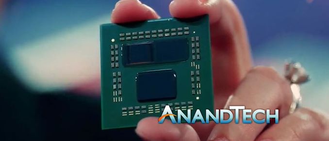
Analysis at Anandtech shows that AMD took TSMC's technology. AMD seems to have confirmed that.
this is clearly TSMC’s SoIC Chip-on-Wafer in action, albeit with only two layers.
In a call with AMD, we have confirmed the following: ... ... AMD knows that TSMC can do multiple stacked dies, however AMD is only talking about a 1-High stack at this time which it will bring to market.


With that said, these are leading-edge packaging technologies, they've been developed with specific customers in mind and may include know-how from those customers. It's not like AMD's purchase manager called TSMC's sales manager and said, hey, we heard you have that, can we have some of it.
 
So if there is any advantage to 3Dfabric for AMD it is thanks to TSMC.
 
So if there is any advantage to 3Dfabric for AMD it is thanks to TSMC.

AMD's innovation was moving to chiplets like 5 years ago, in preparation for this tech to be ready. TSMC is the actual manufacturer though. So of course its TSMC's innovation to actually be able to stich chips together like this. AMD + GloFo were working on this though even as early as Zen1.

Other companies are getting on the chiplet train later than AMD. IBM seems to have been ready for it, NVidia has a bit of usage but not as much as I thought they'd have by now. AMD really went all in on chiplet designs: Zen1, Zen2, Zen3, MI200, etc. etc.

AMD didn't make the physical connections. They just rewrote their protocols to use such connections (aka: Infinity Fabric), which is still a major step forward... albeit a temporary one. (Now that chiplets are proven, everyone else is moving into the space, such as Intel)
 
So if there is any advantage to 3Dfabric for AMD it is thanks to TSMC.
Not sure what your point is? You know who's making the physicals chips, the exotic interconnects or the package right?
 
AMD is just using some TSMC packaging technology that allows stacking of chips. It's not an AMD technology.

They are using it to stack some cache. My thought is that this will be expensive, but we'll see.


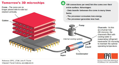
And this concept isn't new (2010) :

 
My point is, the way everyone goes on about this 3D stuff as if AMD came up with it, but they never, it seems it was TSMC. Will they get a TM on the box re 3D stacking or just a fat % off AMD for using it.
 
My point is, the way everyone goes on about this 3D stuff as if AMD came up with it, but they never, it seems it was TSMC. Will they get a TM on the box re 3D stacking or just a fat % off AMD for using it.

AMD has a superb marketing department.

It's probably worth mentioning that the first 3D Stack product was 3D HBM on the Fury GPU. That was 6 years ago IIRC.

Also Intel Lakefield was a Foveros 3D chip.
 
Last edited:
Suppose in the same vein, Intel never actually came up with Big/Little, just their take on it. Is AMD's 3D stack as designed by TSMC or have AMD tweaked it?
 
Suppose in the same vein, Intel never actually came up with Big/Little, just their take on it. Is AMD's 3D stack as designed by TSMC or have AMD tweaked it?

I would imagine that TSMC gave AMD a tool kit for their process node and packaging tech, and AMD used that. I seriously doubt AMD has anything to do with packaging, at least to any large degree - that's the foundry's job. There's an article on AT somewhere that talks about this, but TSMC would literally give like a portfolio or tool kit and from that companies like AMD design their chips. The 'electronics design' of this is ofc on AMD using those tools, but the physics of making the package and the chip is on TSMC. Even the technology that enables 'chiplets' is not AMDs.

So as far as 3D stacking, that's not new. Heat is the main problem, which is why you only see it on something like Lakefield or memory modules so far. Will be interesting to see if / how they solved that.

Heat is the main problem indeed, as the heat from the bottom die has only 1 place to go and that is through the one on top.
 
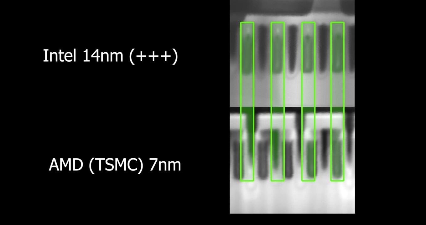
Anyone knows, what is the EXACT ACTUAL dimension of the transistors and transistor gates? For Intel, TSMC and Samsung's?
 
Anyone knows, what is the EXACT ACTUAL dimension of the transistors and transistor gates? For Intel, TSMC and Samsung's?
You'll get at least a part of the answer here
 
Back
Top