Wednesday, September 23rd 2020

Intel 14 nm Node Compared to TSMC's 7 nm Node Using Scanning Electron Microscope
Currently, Intel's best silicon manufacturing process available to desktop users is their 14 nm node, specifically the 14 nm+++ variant, which features several enhancements so it can achieve a higher frequencies and allow for faster gate switching. Compare that to AMD's best, a Ryzen 3000 series processor based on Zen 2 architecture, which is built on TSMC's 7 nm node, and you would think AMD is in clear advantage there. Well, it only sort of is. German hardware overclocker and hacker, der8auer, has decided to see how one production level silicon compares to another, and he put it to the test. He decided to use Intel's Core i9-10900K processor and compare it to AMD's Ryzen 9 3950X under a scanning electron microscope (SEM).
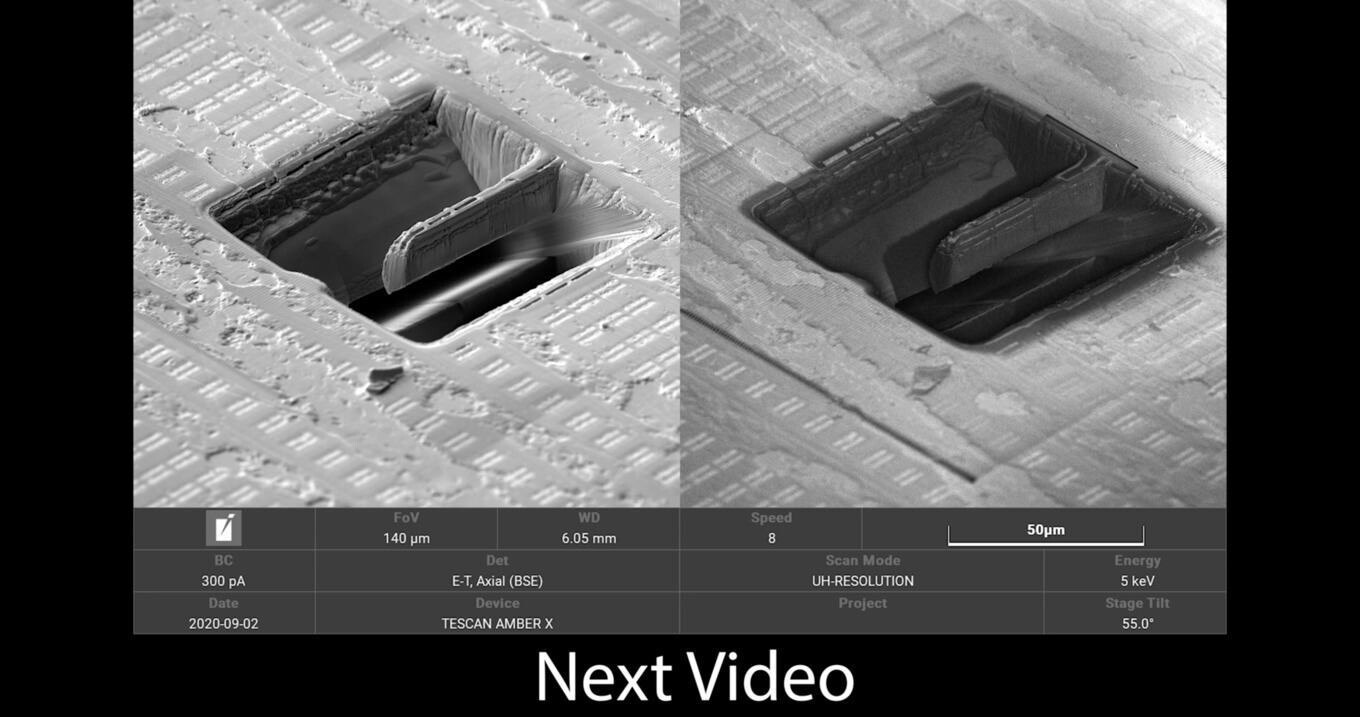
First, der8auer took both chips and detached them from their packages; then he proceeded to grind them as much as possible so SEM could do its job of imaging the chips sans the substrate and protective barrier. This was followed by securing the chips to a sample holder using an electrically conductive adhesive to improve penetration of the high energy electrons from the SEM electron gun. To get as fair a comparison as possible, he used the L2 cache component of both processors as they are usually the best representatives of a node. This happens because the logic portion of the chip differs according to architecture; hence, level two cache is used to get a fair comparison - it's design is much more standardized.
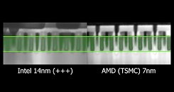

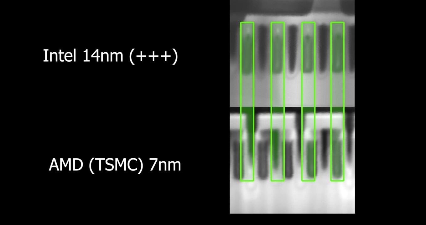
The results? Well, the Intel 14 nm chip features transistors with a gate width of 24 nm, while the AMD/TSMC 7 nm one has a gate width of 22 nm (gate height is also rather similar). While these are not much different, TSMC's node is still much denser compared to Intel's - TSMC's 7 nm produces chips with a transistor density around 90 MT/mm² (million transistors per square millimeter), which is comparable in density to Intel's 10 nm node used on recent mobile processors. Below you can see the SEM images and comparison made. For more information and details please head over to the source.
Another interesting thing to note here, the gate width is not following the naming scheme as you might have expected. The 14 nm transistor isn't 14 nm in width, and the 7 nm transistor isn't 7 nm wide. The naming of the node and actual size of the node have had a departure a long time ago, and the naming convention is really up to the manufacturer - it's become more of a marketing gimmick than anything else. This is the reason researchers have already proposed another density metric for semiconductor technology other than pure "nm" terms.
Source:
Der8auer (YouTube)
First, der8auer took both chips and detached them from their packages; then he proceeded to grind them as much as possible so SEM could do its job of imaging the chips sans the substrate and protective barrier. This was followed by securing the chips to a sample holder using an electrically conductive adhesive to improve penetration of the high energy electrons from the SEM electron gun. To get as fair a comparison as possible, he used the L2 cache component of both processors as they are usually the best representatives of a node. This happens because the logic portion of the chip differs according to architecture; hence, level two cache is used to get a fair comparison - it's design is much more standardized.

Another interesting thing to note here, the gate width is not following the naming scheme as you might have expected. The 14 nm transistor isn't 14 nm in width, and the 7 nm transistor isn't 7 nm wide. The naming of the node and actual size of the node have had a departure a long time ago, and the naming convention is really up to the manufacturer - it's become more of a marketing gimmick than anything else. This is the reason researchers have already proposed another density metric for semiconductor technology other than pure "nm" terms.
49 Comments on Intel 14 nm Node Compared to TSMC's 7 nm Node Using Scanning Electron Microscope
Time to advance in to new materials to get the shrinking going again for real and even get the cost down in the long run.
Today's prices making silicon at 5nm is ridiculous and 3nm will be insane.
All these super computers trying to figure out tomorrows weather should be put to work trying to figure out new materials for making chips instead.
TL;DR Intel is still competitive on the power gating front.
Proof reading please.
We kinda knew this since Ivy Bridge, 22nm, when increased heat concentration would put pressure on the IHS/TIM solution, neutering OC potential. Ever since AMD adopted 7nm for its CPUs, they're seeing similar stuff.
Nonetheless its nice to see it from this angle and with the current state of things, seeing as Intel added all those pluses.
The TL DR here is that over the past half decade, in spite of glorious marketing, the best we can say is we've made a tiny baby step forward from 14nm's first iteration. Sounds depressing if you think of the artillery that was used to get here... OTOH, it also means we've still got ground to cover.You think this is bad? Lol. Welcome to TPU. Get used to it;)
Next time if you want corrections its a better idea to send the poster a PM or tag them in your reply with @
In the end what really matters is performance per Watt.
Intel's main problem is not their node, never has been. It's sitting on the Skylake arch for too long. Going to Tiger Lake will change up the map on mobile, provided they can get quantity out.
I think Rocket Lake, despite being "14nm", will also be a significant part in terms of performance. It's basically a high frequency Tiger Lake without the Xe graphics. This article just reinforces that view.