Friday, September 11th 2009

AMD Cypress ''Radeon HD 5870'' Stripped
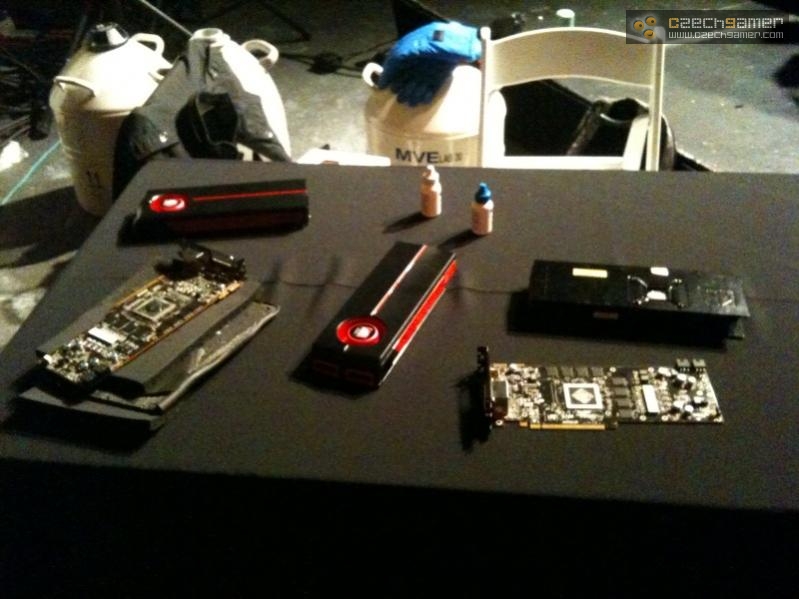
Here are the first pictures of the obverse side of Cypress' PCB, and the first pictures of the centre of attraction: the AMD Cypress GPU. CzechGamer dissembled two Cypress "Radeon HD 5870" cards for a quick blurrycam photo-session. The PCB shot reveals quite a bit about Cypress, particularly about the GPU.
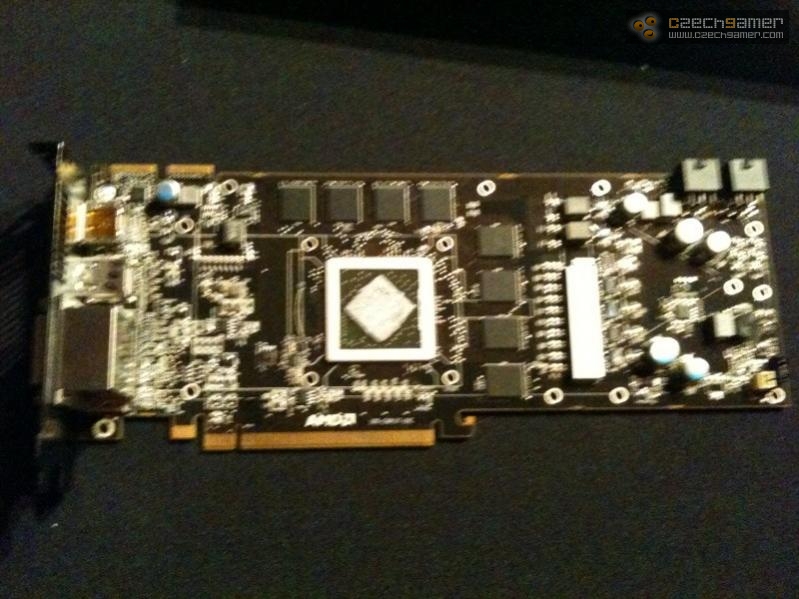
To begin with, the GPU is AMD's overhaul on transistor counts, and a bold work of engineering on the 40 nm manufacturing process, given the kind of problems foundry partners had initially. Apparently they seem to have recovered with most of them, as AMD's AIB partners are coming up with new products based on the 40 nm RV740 GPU on a weekly basis. The package holds a "diamond-shaped" die that is angled in a way similar to RV740, RV730, or more historically, the R600. The seemingly huge die measures 338 mm² (area), and for 40 nm, it translates to "huge", and is vindicated by the transistor count of ~2.1 billion. In contrast, AMD's older flagship GPU, the RV790 holds 959 million, and NVIDIA's GT200 holds 1.4 billion. The PCB has three distinct areas: the connectivity, processing, and VRM. To fuel the GPU is a high-grade 4 phase digital PWM power circuit, while the PCB has placeholders for an additional vGPU phase. The 8 (or 16 on the 2 GB model) memory chips, is powered by a 2 phase circuit. Power is drawn from two 6-pin PCI-Express power connectors, but there seems to be a placeholder for two more pins, i.e., to replace one of those 6-pin connectors with an 8-pin one. Bordering the GPU on two sides are the 8 GDDR5 memory chips, which AMD calls says is generation ahead of present GDDR5, and supports reference frequencies as high as 1300 MHz (2600 MHz DDR, 5.20 GHz effective). In the 2 GB variant, 8 more chips seat on the other side of the PCB. This is what perhaps, the backplate is intended to cool. On the connectivity portion of it, are the two CrossFire connectors, DisplayPort, HDMI and a cluster of two DVI-D connectors. There has been a raging debate about how adversely the small air vent would affect the card, but AMD is promising some energy efficiency breakthroughs, plus given how roomy the card is, the vent seems sufficient.

Finally, information from ArabHardware.net suggests a pricing model on three of the first SKUs based on Cypress: HD 5870 2 GB, HD 5870 1 GB, and HD 5850 1 GB. All three use the same GPU and memory standard (GDDR5), but differ in clock speeds and GPU configurations. While HD 5870 sports 1600 stream processors, 80 TMUs, and 32 ROPs, HD 5850 has 1440 stream processors, 72 TMUs, and 32 ROPs. Although 32 ROPs puzzles us for a 256-bit wide memory interface, we suspect low-level design changes that make "32 ROPs" more of an effective count than an absolute count. While HD 5870 features over 800 MHz core clock and 5.20 GHz memory, its little sibling has over 700 MHz core clock and 4.40 GHz memory. Price points expected are US $449 for Radeon HD 5870 2 GB, $399 for HD 5870 1 GB, and $299 for HD 5850. AMD is expected to announce all three models on the coming 23rd. You'll be able to find them at your favourite computer store a little later, availability is a certainty by the time you're ready to buy Windows 7. AMD's newest products will be more than ready to squat under X-mas trees all over.
Sources:
Czech Gamer, Arab Hardware
To begin with, the GPU is AMD's overhaul on transistor counts, and a bold work of engineering on the 40 nm manufacturing process, given the kind of problems foundry partners had initially. Apparently they seem to have recovered with most of them, as AMD's AIB partners are coming up with new products based on the 40 nm RV740 GPU on a weekly basis. The package holds a "diamond-shaped" die that is angled in a way similar to RV740, RV730, or more historically, the R600. The seemingly huge die measures 338 mm² (area), and for 40 nm, it translates to "huge", and is vindicated by the transistor count of ~2.1 billion. In contrast, AMD's older flagship GPU, the RV790 holds 959 million, and NVIDIA's GT200 holds 1.4 billion.

163 Comments on AMD Cypress ''Radeon HD 5870'' Stripped
Majorly want to get my mits on a 2gb Eyefinity 5870
www.amd.com/us/products/technologies/eyefinity/Pages/eyefinity.aspx
1) Driver version 8.66 (Catalyst 9.10) or above is required to support ATI Eyefinity technology and to enable a third display you require one panel with a DisplayPort connector.
So either this means they worked Eyefinity into the drivers a long time ago, or that this is mainly a hardware tweak on the Evergreen cards. But it almost certainly means that Eyefinity will not be available on older cards (4xxx series for example). The other interesting bit is that fact that it requires DisplayPort for more than two displays. I think that is why all the demos used those displayport to DVI(?) adaptors
image source part of LegitReview article
www.techpowerup.com/?101730
shows 2 DVI, 1 DisplayPort, 1 HDMI which I think will be the standard configuration. So three display Eyefinity with 2DVI +1DisplayPort or DVI+HDMI+DisplayPort but not 2DVI+HDMI. At least that is what the fine print is implying.
The big question is whether a DisplayPort->DVI cable will allow 3 DVI monitors to do 3way Eyefinity?
This version above (presumably the 2GB version) shows a full slot of exhaust, not a narrow one like in some other pictures..
Well, if the final "reference" board is going to ship with a narrow exhaust slot opening, then I guess it would be because the card is indeed going to run cool enough after all. I can vividly remember my X1900XTX exhausting a strong flow from its noisy stock cooler out the left half of the exhaust opening, while I hardly felt any airflow from the right half of the opening. I replaced the cooler with a HIS IceQ Turbo cooler anyways, which did a quieter job of cooling that insanely hot/power-hungry chip.
the cards haven't even come out of NDA
Just one process node shrink from 55nm to 40nm (of which the INQ argues to actually be 45nm, but now they call it "40/45nm"), and we're seeing 2x the specs at a LOWER power consumption, using the same clocks. The chip die size area is actually more than 2x as big as a virtual 4890 shrunk to 40nm.
It must be an incredible design job done by ATI. Remember how Nvidia's shrink from 65nm to 55nm almost did nothing with respect to power savings (maybe 15W at the most)?
What I am guessing is that the 5870 runs at an incredibly low voltage for ATI to be making an announcement of only 188W TDP (after they announced a 190W TDP for their 4890). The 40nm spin must have been so successful that it was a breeze clocking their cores at 850MHz, at say, 1.1v or so. Also, I can recall ATI stating that they would ensure their future GPU to be completely error free according to Tetedeiench 's new OCCT GPU stress-testing tool, so I would expect ATI to be a bit more serious about the power consumption figures that they announce (in that the 5870 would not be as power-hungry as a 4890).
I would guess that it means we can overclock the HELL outta this thing!!! Increasing it to say, 1.3 or 1.4v could yield 1.1GHz or more for stable operation... hopefully!! :rockout::rockout::rockout: