Tuesday, August 24th 2010

AMD Details Bulldozer Processor Architecture
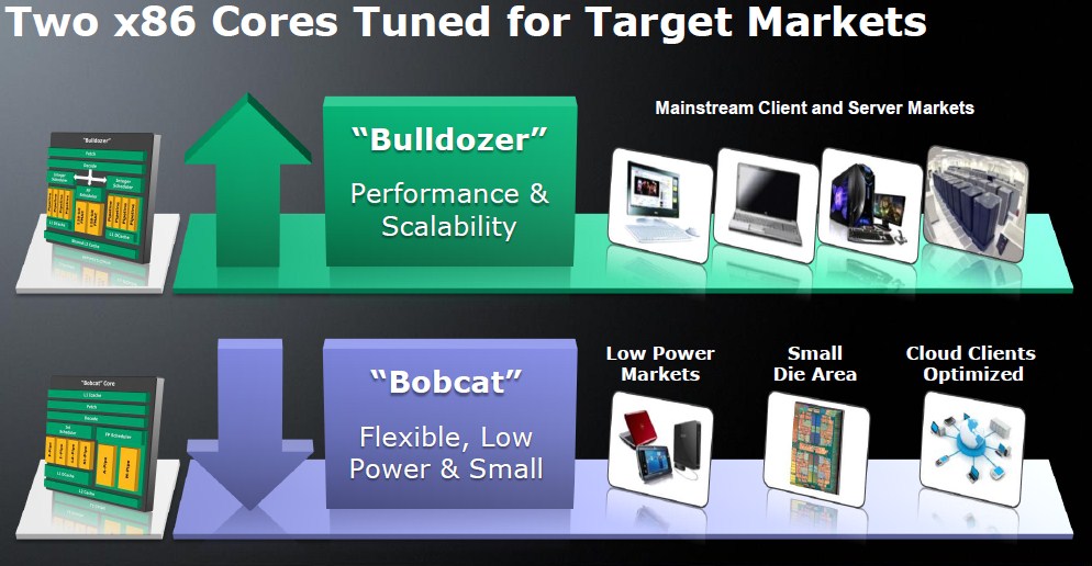
AMD is finally going to embrace a truly next generation x86 processor architecture that is built from ground up. AMD's current architecture, the K10(.5) "Stars" is an evolution of the more market-successful K8 architecture, but it didn't face the kind of market success as it was overshadowed by competing Intel architectures. AMD codenamed its latest design "Bulldozer", and it features an x86 core design that is radically different from anything we've seen from either processor giants. With this design, AMD thinks it can outdo both HyperThreading and Multi-Core approaches to parallelism, in one shot, as well as "bulldoze" through serial workloads with a broad 8 integer pipeline per core, (compared to 3 on K10, and 4 on Westmere). Two almost-individual blocks of integer processing units share a common floating point unit with two 128-bit FMACs.
AMD is also working on a multi-threading technology of its own to rival Intel's HyperThreading, that exploits Bulldozer's branched integer processing backed by shared floating point design, which AMD believes to be so efficient, that each SMT worker thread can be deemed a core in its own merit, and further be backed by competing threads per "core". AMD is working on another micro-architecture codenamed "Bobcat", which is a downscale implementation of Bulldozer, with which it will take on low-power and high performance per Watt segments that extend from all-in-One PCs all the way down to hand-held devices and 8-inch tablets. We will explore the Bulldozer architecture in some detail. Bulldozer: The Turbo Diesel Engine
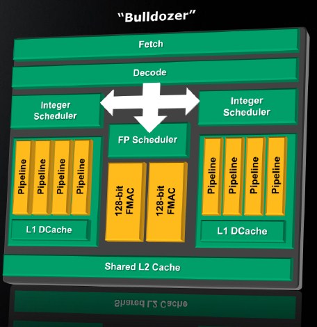
In many respects, the Bulldozer architecture is comparable to a diesel engine. Lower RPM (clock-speeds), high torque (instructions per second). When implemented, Bulldozer-based processors could outperform competing processor architectures at much lower clock speeds, due to one critical area AMD seems to have finally addressed: instructions per clock (IPC), unlike with the 65 nm "Barcelona" or 45 nm "Shanghai" architectures that upped IPC synthetically by using other means (such as backing the cores up with a level-3 cache, upping the uncore/northbridge clock speeds), the 32 nm Bulldozer actually features a broad integer unit with eight integer pipelines split into two portions, each portion having its own scheduler and L1 Data cache.
Parallelism: A Radical Approach?
Back when analysts were pinning high hopes on the Barcelona architecture, their hopes were fueled by early reports suggesting that AMD was using wide 128-bit wide floating point units, leading analysts to believe that AMD may have conquered its biggest nemesis - floating point performance, in turn its pure math crunching abilities. However, that wasn't exactly to be. That's because the processor's overall number crunching abilities were pegged to its floating point performance, ignoring the integer units.
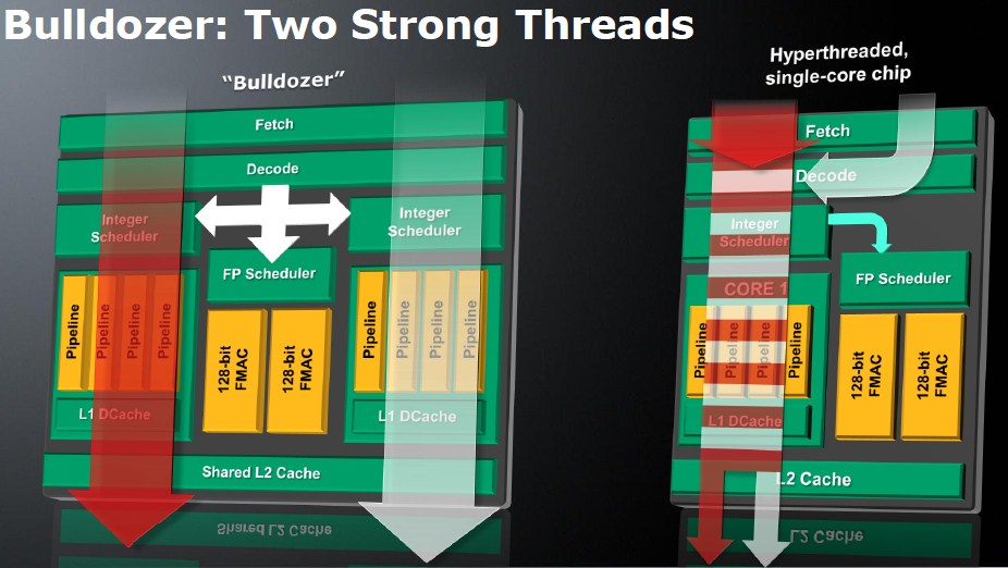
AMD split 8 integers per core into two blocks, each block having four integer pipelines, an integer scheduler for those, and an L1 Data cache. These constitute the lowest level of "dedicated components", dedicated to processor threads. There is a shared floating point unit between the two, with two 128-bit FMACs, arbitrated by a floating point scheduler. The Fetch/Decode, an L2 cache, and the FPU constitute "shared" components.
AMD is implementing a simultaneous multithreading (SMT) technology, it can split each of the "dedicated" components (in this case, the integer unit) to deal with a thread of its own, while sharing certain components with the other integer unit, and effectively make each set of dedicated components a "core" in its own merit of efficiency. This way, the actual core of the Bulldozer die is deemed a "module", a superlative of two cores, and the Bulldozer die (chip) features n-number of modules depending on the model. So now you have a chip with eight cores with much lower die sizes and transistor counts compared to a hypothetical 32 nm K10 8-core processor. It is unclear whether AMD wants to further push down SMT to the "core" level and run two threads simultaneously over dedicated components, but one thing for sure is that AMD has embraced SMT in some form or another. In all this, the chip-level parallelism is transparent to the operating system, it will only see a fixed number of logical processors, without any special software or driver requirement.
So in one go, AMD shot up its integer performance. Either a thread makes use of one integer unit with its four pipelines, or deals with both the integer units arbitrated by the fetch/decode, and the shared FPU.
Outside the modules
At the chip-level, there's a large L3 cache, a northbridge that integrates the PCI-Express root complex, and an integrated memory controller. Since the northbridge is completely on the chip, the processor does not need to deal with the rest of the system with a HyperTransport link. It connects to the chipset (which is now relegated to a southbridge, much like Intel's Ibex Peak), using A-Link Express, which like DMI, is essentially a PCI-Express link. It is important to note that all modules and extra-modular components are present on the same piece of silicon die. Because of this design change, Bulldozer processors will come in totally new packages that are not backwards compatible with older AMD sockets such as AM3 or AM2(+). Expectations
Not surprisingly, AMD isn't talking about Bulldozer as the next big thing since dual-core processors (something it did with Barcelona). AMD currently does have an 8-core and 12-core processors codenamed "Magny-Cours", which are multichip modules of Shanghai (4-core) and Istanbul (6-core) dies. AMD expects an 8-core Bulldozer implementation (built with four modules), to have 50% higher performance-per-watt compared to Magny-Cours.
Market Segments
As mentioned in the graphic before, AMD's modular design allows it to create different products by simply controlling the number of modules on the die (by whichever method). With this, AMD will have processors ready with most PC and server market segments, all the way from desktop PCs, enthusiast-grade PCs, notebooks, to servers. AMD expects to have a full-fledged lineup in 2011. The first Bulldozer CPUs will be sold to the server market.
AMD is also working on a multi-threading technology of its own to rival Intel's HyperThreading, that exploits Bulldozer's branched integer processing backed by shared floating point design, which AMD believes to be so efficient, that each SMT worker thread can be deemed a core in its own merit, and further be backed by competing threads per "core". AMD is working on another micro-architecture codenamed "Bobcat", which is a downscale implementation of Bulldozer, with which it will take on low-power and high performance per Watt segments that extend from all-in-One PCs all the way down to hand-held devices and 8-inch tablets. We will explore the Bulldozer architecture in some detail.
In many respects, the Bulldozer architecture is comparable to a diesel engine. Lower RPM (clock-speeds), high torque (instructions per second). When implemented, Bulldozer-based processors could outperform competing processor architectures at much lower clock speeds, due to one critical area AMD seems to have finally addressed: instructions per clock (IPC), unlike with the 65 nm "Barcelona" or 45 nm "Shanghai" architectures that upped IPC synthetically by using other means (such as backing the cores up with a level-3 cache, upping the uncore/northbridge clock speeds), the 32 nm Bulldozer actually features a broad integer unit with eight integer pipelines split into two portions, each portion having its own scheduler and L1 Data cache.
Back when analysts were pinning high hopes on the Barcelona architecture, their hopes were fueled by early reports suggesting that AMD was using wide 128-bit wide floating point units, leading analysts to believe that AMD may have conquered its biggest nemesis - floating point performance, in turn its pure math crunching abilities. However, that wasn't exactly to be. That's because the processor's overall number crunching abilities were pegged to its floating point performance, ignoring the integer units.


So in one go, AMD shot up its integer performance. Either a thread makes use of one integer unit with its four pipelines, or deals with both the integer units arbitrated by the fetch/decode, and the shared FPU.
Outside the modules
At the chip-level, there's a large L3 cache, a northbridge that integrates the PCI-Express root complex, and an integrated memory controller. Since the northbridge is completely on the chip, the processor does not need to deal with the rest of the system with a HyperTransport link. It connects to the chipset (which is now relegated to a southbridge, much like Intel's Ibex Peak), using A-Link Express, which like DMI, is essentially a PCI-Express link. It is important to note that all modules and extra-modular components are present on the same piece of silicon die. Because of this design change, Bulldozer processors will come in totally new packages that are not backwards compatible with older AMD sockets such as AM3 or AM2(+).

Not surprisingly, AMD isn't talking about Bulldozer as the next big thing since dual-core processors (something it did with Barcelona). AMD currently does have an 8-core and 12-core processors codenamed "Magny-Cours", which are multichip modules of Shanghai (4-core) and Istanbul (6-core) dies. AMD expects an 8-core Bulldozer implementation (built with four modules), to have 50% higher performance-per-watt compared to Magny-Cours.

As mentioned in the graphic before, AMD's modular design allows it to create different products by simply controlling the number of modules on the die (by whichever method). With this, AMD will have processors ready with most PC and server market segments, all the way from desktop PCs, enthusiast-grade PCs, notebooks, to servers. AMD expects to have a full-fledged lineup in 2011. The first Bulldozer CPUs will be sold to the server market.
283 Comments on AMD Details Bulldozer Processor Architecture
*edit*
With faster ram as far as i knew the only time you would see a big improvement is when something needs more bandwidth than is available, i only want so much bandwidth to go with 6 or 8 cores and multiple virtual machines to run 24/7 while carrying on all other normal usage.
I'm with Wile E on this one, I want the best components for my rig(s) and if Bulldozer can compete with Intel on both performance and then it'll be my next purchase. I'm also hoping AMD have some fight in them and if the deal with Apple is true, then that'll be some much needed revenue that'll hopefully give them more resources to make all the right moves resulting in more competitive prices for the consumer... me!
:D
Here's an DDR2 OCZ kit of memory with cas 5 timings: www.amazon.com/dp/B0017SA5ZY/?tag=tec06d-20
And here's the DDR3 version of that same kit with higher speed but still higher timings (cas 7): www.amazon.com/dp/B0013HC36S/?tag=tec06d-20
Still fairly high from what im looking at, which DDR3 kits are lower?
Timings =! latency
DDR3 1600 CAS 9 has a lower latency then DDR3 1333 CAS 9 because the speed (in nanoseconds) of DDR3 1600 is 1.25 and DDR3 1333 is 1.50 hence you get 10.5ns for 1600 and 13.5ns for 1333.
DDR2 666 CAS 4 has a latency of 12ns because the speed of the dimm is twice that of DDR3 1600 at 3ns.
Secrets of PC Memory
Read that and understand this:
DDR refresh clock (tCLK):
DDR 200 is 10.0ns
DDR 266 is 7.52ns
DDR 333 is 6.02ns
DDR 400 is 5.00ns
DDR2 refresh clock (tCLK):
DDR2 400 is 5.00ns
DDR2 533 is 3.76ns
DDR2 667 is 3.00ns
DDR2 800 is 2.50ns
DDR2 1066 is 1.876ns
DDR3 refresh clock (tCLK):
DDR3 1066 is 1.876ns
DDR3 1333 is 1.50ns
DDR3 1600 is 1.25ns
DDR3 1866 is 1.07ns
DDR3 2000 is 1.00ns
To find the latency of any dimm you need to take its tCLK and multiply it by its listed timings to find the latency of that timing.
DDR3 is worth it to me just because it is getting cheap, and it runs a lot cooler.
Sure some programs wont even have improvement at all.
But tbh an fair it's better to increase your storage transfer rates before your memory.
Again I'm not 100% on that part but it is from what I've come to understand from what I've read. I'm not 100% on why the way the data is retrieved has anything to do with the size limit of the dimm.
If any one wants to make their mind bleed from trying to understand memory read: Everything you always wanted to know about sdram memory but were afraid to ask on Anandtech. Also their article ASUS ROG Rampage Formula: Why we were wrong about the Intel X48 may need reading first to be able to follow along in the other.
I got to about page 4 before I said f- this and then got saved on page 5 with the Youtube video. I kind of skimmed from there because it was stretching my mind mentally trying to follow along.
now i use 1600mhz 6-8-6-24 modules DDR3 triple channel, and they keep Cas6 untill 1800mhz... and Cas7-8 @ 2000mhz ...
You can 't compare latencies using CAS between different type of memory, DDR1-2-or 3 .... it's a false idea.
for give you an idea: Sandrasisoftware give me a 29go/s bandiwth with my DDR3@1600mhz ( CPU@200x20).... how much you have with DDR2 ? 15go/s? ( this have nothing to do with latencies, but well it's just for information )
Best quote:The DDR3 article mixes latency with dimm clock cycles (tCLKmin) needed to complete an action (CAS, RAS, etc). This would only be true if tCLKmin was equal to 1ns, but that only happens at 2000mhz for DDR3. Just 2 paragraphs later they get it right:The first part should say "typical timings" instead of "typical latencies" because it makes it sound like 5-5-5-15 is the latency but its not. Its just the number of cycles need to complete that action at the given speed (i.e 800mhz for ddr2). The latency changes once the speed goes to 1066mhz for DDR2 and it would be a mistake to say 5-5-5-15 equals latencies.
Example:
DDR2 Timings of 5-5-5-15 at
-------------------------------------------------
1066mhz is about 9.5 - 9.5 - 9.5 - 28 (in nanoseconds)
800mhz is about 12.5 - 12.5 - 12.5 - 37.5 (in nanoseconds)
DDR3 Timings of 7-7-7-20 at
-----------------------------------------------------
1066mhz is about 9.5 - 9.5 - 9.5 - 28 (in nanoseconds)
1333mhz is about 10.5 - 10.5 - 10.5 - 30 (in nanoseconds)
This also shows that not only is 1066 DDR3 marginally faster (then 1333 DDR3) given those timings but, unless you have some bandwidth sensitive real world application, there is no real gain by going to 2000mhz DDR3 CAS 9 dimms when the latencies between the two are almost the same. The difference only shows up if the program moves a lot of data in and out of memory otherwise its just wasted (as in most cases). This is also why lower the refresh (tREF) makes the system "feel" fast and more responsive because the system is waiting less and less for the data to be refreshed and minimal changes show up quicker.
If anything maybe that last post adds something I missed in the other one. :laugh: