Monday, September 6th 2010

Picture of AMD ''Cayman'' Prototype Surfaces
Here is the first picture of a working prototype of the AMD Radeon HD 6000 series "Cayman" graphics card. This particular card is reportedly the "XT" variant, or what will go on to be the HD 6x70, which is the top single-GPU SKU based on AMD's next-generation "Cayman" performance GPU. The picture reveals a card that appears to be roughly the size of a Radeon HD 5870, with a slightly more complex-looking cooler. The PCB is red in color, and the display output is slightly different compared to the Radeon HD 5800 series: there are two DVI, one HDMI, and two mini-DisplayPort connectors. The specifications of the GPU remain largely unknown, except it's being reported that the GPU is built on the TSMC 40 nm process. The refreshed Radeon HD 6000 series GPU lineup, coupled with next-generation Bulldozer architecture CPUs and Fusion APUs are sure to make AMD's lineup for 2011 quite an interesting one.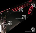
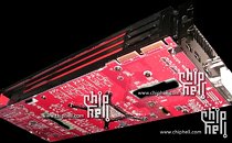
Update (9/9): A new picture of the reverse side of the PCB reveals 8 memory chips (256-bit wide memory bus), 6+2 phase VRM, and 6-pin + 8-pin power inputs.
Source:
ChipHell


118 Comments on Picture of AMD ''Cayman'' Prototype Surfaces
fermi consume 320w was because it added a lot of non gaming particle(general computing) which waste hugely on die size. if they could take it off the power rate will drop 30%....
tell me why 512bit is cost a lot first. it might cost a lot back in r600 with pathetic 80nm fab but today this will be solve thanks to 40nm process mostly because r600 only had 16 rops which most of bus width were wasted. but today a cypress has 32rops thing goes different. each rops only share 8bit per length. but 32rop is still enough to fit in 256bit bus(barely...). but what happen if a gpu that has 64rop? it will cause bottleneck in communication between gpu and ram. it doesn't matter overall bandwidth if most of data stuck at rops due to the narrow bus width. for example a cypress xt suppose to be double of rv770xt in every spec but end up only 55% increase in performance. while rv770xt is about double of rv670 in every bench? why cause such difference? the answer, the bus width can't feed enough of data length to GPU rops/shaders. a 512bit is necessary for future gpu that have more rops/shadersource? :Dagain tell me why 512bit cost a lot? because of bad experience from r600?
do you think a a $599 card for high end is expansive?
larger bus means more pins more pins means more complex the more complex the more likely of failure higher failure rate of a die means lower yield lower yield means less profit
also the pins can only be so small before there to brittle to solder to a PCB meaning a 512bit = more pins and the pins can only get so small before they cant be shrunk down meaning 512bit takes more space
so all a 512bit does effectively for todays GDDR5 is
*give bandwidth the gpu cant use
*makes a more complex PCB design
*has a higher risk of failure due to complexity
source read this article and learn something
www.extremetech.com/article2/0,2845,2309870,00.asp\
a perfect example of why 512isnt needed
4850 vs 4870 despite double the bandwidth from GDDR3 to GDDR5 the 4870 is only 20% faster the ram nor ram speed made the difference it was the higher core clock as the to cards used the same gpu just different ram to no real benefit.
same can be said of 256bit vs 512bit a 4870 could have a 512bit interface but if it uses GDDR3 its only equal to GDDR5 at 256bit what this means is the 512bit was more complex to produce but had no benefit over the cheaper bus with faster lower voltage memory
what this means is even if you double the bus width and the bandwidth it wont make a 6870 any faster to warrant the cost of the design. now you can have your opinion but last i checked you werent an Engineer working for Nvidia or ATi and seem to have no understanding of this subject in anyway to form a decent and well informed opinion on it nor are you able to see the big picture in the design of the GPU
"Just because you can dosent mean you should" is what comes to mind in terms of 256bit vs 512bit
another way to see it is you lose 10% overall wafer space so you get 10% less GPUs per wafer but gain 5% in performance that 5% gain dosent make you more money because the 5% gain from 256bit to 512bit is something they can get in a cheaper more cost effective way. So basically if a wafer provides 100gpus at 256bit and 95% performance and 512bit offers 90gpus at 100% performance if we count that in terms of products to market sure it might only be $20 on the manufacturing end but if those are wafers of $700 gpus those extra 10gpus just earned said company an extra $7000 per 100gpus at 256bit vs 90 at 512bit thats why you wont see 512bit.
becuase 1,000,000 gpus vs 900,000 if all of them are full functional is a huge profit difference for companies not to mention the 1m gpus at 256bit will most likely have higher yield then 512bit means in terms of usable GPUs
the 1m might be 800,000 that can be used but the 900k might only be 600k usable so by the time you run the numbers your precious 512bit costs millions in profit. These companies are not here to hold your hand thats your mothers job there here to make money 512bit wont make them any more money then 256bit it infact costs more and since ATi/AMD is trying to maintain a Positive cashflow means there going to take the tiny insignificant 1 fps loss in crysis between 256 and 512 and reap an extra $20 instead
note my math is hypothetical i dont know the actual manufacturing costs of the GPU itself and all components but im sure most around here will agree the logic itself is what matters and its solid
This thread turned into a memory bus discussion. IMHO, the bus doesn't matter, you don't get anything having for example a 512 bit bus with a 400MHz DDR2 memory, what matters is the GDDR5 clock in this case, so AMD can stick to a cheaper 256 bit bus and clock the memory higher. Then I'd say GDDR5 clocked to 1500 MHz on a 256 bit bus (192 GB/s) is my safe bet.
larger bus require more pin on the bga board that contain gpu. indeed but it doesn't really give any further die increase and nothing to do with die/wafer. just the board become more complex and more layer for pcb board and increase size of gpu footprint, but not die size. the source also didn't mention it will cause lower yield on gpu die. mostly it would just cause difficulty to graphic card manufacturer to design the board. amd didn't lose any profit because this is just for high end part exclusively. and eventually neither nvidia and amd can go without bigger bus in future.then remove some unnecessary design such as 5D shader and stop adding more shader like what they did in r700...they were wasted far more die space by putting these additional float point feature(again like fermi....for that stupid general compute and that stupid fold@home?) if they cut it off they could have save a lot of die space to stuff more feature for pure performance....though i think they did make some new tweak on southern islands by tried to remove as much of those useless feature and bring back what graphic card suppose to be- rendering graphic.. r600's massive shader architecture was one of worst way to improve performance.48rops means "half note" design....that is why fermi fall so bad
afterall why would they make the 6000 series even more expensive to produce when they will most likely only be around for 10months - a year much like the 5k cards before there replaced by the 7000 series which will be an all new architecture from the ground up it makes no sense to have a stop gap gpu cycle cost any more then is needed to hold there market share and keep Nvidia in check
wow, i never expect this card com out so quickly,
an ancient wisdom "if you can't make history, you will be abandon by history"
PS: oh just right after the discussion when i was about to bring evidence of 512bit from wiki and somebody just had to erase it and mess the whole article. wow. crazy if you are part of hack group you are in seriously trouble. wikipedia is under investigate. didn't realize someone just cant take the truth lol
AMD has said several times why they won't do it. You should read the two Anandtech articles about the 4 and 5 series if you havn't.
To use 3 monitors, you'd still have to convert the mini-DP to DVI, since using 2 DVI ports disables the HDMI, leaving only the 2 DP ports.
1: 2x wiring on the PCB
2: 2x memory chips
3: get rid of EMI,which will make u hit higher clocks,
4: so its allot cheaper and less complex PCB
see why the 460 can hit higher memory speed than 480 cuz its less complex con the memory controller side and the PCB side
and if they make 384bit it wouldn't hit 6400mhz easily would it ??
check this out if its real it will:nutkick: nvidia:D
forums.anandtech.com/showpost.php?p=30402647&postcount=497
this had been said so many time that cayman is for high end market. so so it has to be 64rops~128rops/3D~4Dshader/512bit bus and it will cut off many of unused shader off from cypress design. PCB layout and wiring cost would not be consider. unless you want to buy a crappy "high end" like 4870 that couldn't even compete 8800gtx in 70% of games. these useless shader only work on game that based on unreal 3 engine, but again unreal 3 engine is shit and only exclusive for console. like i said before if they get rip of 5D shader and make it 4D or even 3D shader and turn it to pure gaming card will save plenty of space.
gtx 460 hit higher ram clock was because they want to grab back some market share which force them to do so, and mostly done by overclock and overvoltage because they can't get faster ram. this is not because of "cuz its less complex con the memory controller side and the PCB side " it was because nvidia hasn't been license yet to integrate faster GDDR5 ram and yet amd and hynix holding the GDDR5 patent as long as amd no authorize, nvidia/gtx480 will never get any faster ram. and these memory controller/pcb layout cost only be consider in mid range board so obviously GTX460 is doing a correct move. but it's not correct if on upcoming gtx 485.... if hynix can license nv with faster ram like amd and with its wider bus fermi will destroy any future line of radeon if that are still continue that pathetic r600 design.
if a 6770(barts) is a revolutionary design then why not cayman be a revolutionary design as well? unless you telling me they are enjoy their success and try get more milk than put out better product like good old k8/r300 day. no wonder amd/ati are always be a secondary company...
Sapphire have a special 5770 flex model that can use 3 DVI monitors and no active adapters.
www.pccasegear.com/index.php?main_page=product_info&cPath=193_962&products_id=15368
and you seem to like talking about r 600 and r 300 what about the g92 lol been in use for nearly 4 years with no re improvement where as ati has scaled there design to offer better performance you can argue your points all you want because fact is the biggest baddest gpu nvidia had which was the 512 shader gtx 480 was only 5% faster then the 480 shader current high end both companies have room for improvement. and how is the r600 design pathetic? last i checked the 5850 5870 and 5970 are highly competitive compared to nvidias offerings and in general use nearly 35-40% less power to do so and if its truly fail then why did Nvidia lose so much market share to this pathetic design?
fermi consume 40% more power and 50% larger die size was because of too many non addon feature(GPGPU). if they can remove it amd will be in seriously trouble. if gtx 480 is no longer a gpgpu the die size will shrink at least 40% while keep the same spec. you seem don't understand how important rops and bus would cause huge performance hit don't you? yeah of cause gtx 480 is still second pace in single card solution. but don't forget this, dual gpu PCB cost about twice as much as a GTX480 can be. the wiring is far far complex than any of single gpu board content. let me tell you this a gtx 480 board is far cheap than hamlock XT board the only disadvantage was die size that's all. if amd insist making only dual gpu board they'd have to consider more cost in layout than an "UNNECESSARY" 512bit bus board can be. GTX460's case is more like 5830, it cut off many feature while didn't optimize transistor make it more inefficient on its die size(a 324mm^2 "cripple" die would generate power of 400mm^2 which seem logical).
you keep talking how well r600 art is while ignore the fact they sacrifice the performance for saving production cost. g92 came out at november 2007 which is not even 3 years yet where did you get the idea of 4 years? even g92 is old but not even hd 4800/5770 still cant even out pace g94 in tremendously margin and gts 250 is on the side compete with 4850 and amd still couldn't get and better midstream product to outcast old g92 line :D where were amd doing these year :D and nvidia did lose share only because of discontinue of g92/g94 line while there are no product to replace it. they only lose a bit because of school opening season and they have nothing to sell. not because of fermi. and yet r600 IS a pathetic design no matter you agree or not.