Friday, November 12th 2010

Radeon HD 6900 Series Officially Postponed to Mid-December

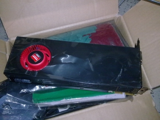
Originally poised for a November 22 launch, and plagued by reported delays, the Radeon HD 6900 series from AMD is indeed staring down at a three-week delay. According to a new release by AMD circulated to press sites, AMD is pinning the new launch date to be "in the week of" December 13, 2010. AMD tried to explain that the Radeon HD 5800 series is still in strong demand, and the Radeon HD 5970 is still maintaining performance leadership, perhaps blaming congestion in inventories for the delay, and not anything to do with manufacturing.

The first part of the explanation is unconvincing. If AMD did not want to disturb Radeon HD 5800 series sales, there wouldn't be Radeon HD 6800 series, which was launched with the idea of giving HD 5800-like performance at more affordable prices. The second part, however, is hard to dispute. AMD signed off its release saying that enthusiasts will find the products worth the wait. December 13, however, could disturb some gifting (or self-gifting) plans for Xmas. Given the swamped courier and logistics services at that time, it will be tough to get a Radeon HD 6900 series product in time for the celebrations.
Add your own comment

52 Comments on Radeon HD 6900 Series Officially Postponed to Mid-December

#26
yogurt_21
mdsx1950DAMMIT!

I was waiting to get a 6900 card before December. WTF?
yeah but you were going for the 6990 and that was already posponed until january.
Posted on Reply
#27
NdMk2o1o
LAN_deRf_HAAt this point there's been so many rumors the only way we'll ever know the real reason for the delay is if AMD tells us
........
btarunrAccording to a new release by AMD circulated to press sites
From the horses mouth.
Posted on Reply
#28
mdsx1950
yogurt_21yeah but you were going for the 6990 and that was already posponed until january.
Nope i was going for 4x 6970s. :p :rockout:
Posted on Reply
#29
btarunr
Editor & Senior Moderator
function69At this point it's prolly too late to make any hardware changes, just in software (drivers) and you can only do so much with those.
You definitely can change the GPU specs (with increased clocks, if the cooler permits). NVIDIA did just that after it found out that its original GTX 480 was too slow after the Radeon HD 5000 series released, but had to also redesign the cooler to keep up with the increased clock speeds (which added to the development time).
Posted on Reply
#30
Fourstaff
mdsx1950DAMMIT!

I was waiting to get a 6900 card before December. WTF?
Well, you will certainly get your card before Dec 2011 :p
Posted on Reply
#31
mdsx1950
FourstaffWell, you will certainly get your card before Dec 2011 :p
:mad: Not funny
:p :laugh:
Posted on Reply
#32
Unregistered
btarunrYou definitely can change the GPU specs (with increased clocks, if the cooler permits). NVIDIA did just that after it found out that its original GTX 480 was too slow after the Radeon HD 5000 series released, but had to also redesign the cooler to keep up with the increased clock speeds (which added to the development time).
so do you think that nvdia think more Mghz was more important than more SP?
#33
CDdude55
Crazy 4 TPU!!!
That sucks.:(
Posted on Reply
#34
btarunr
Editor & Senior Moderator
wahdangunso do you think that nvdia think more Mghz was more important than more SP?
More MHz needs a lower power budget than More SPs. With GF110, (of which NV didn't release an architecture schematic till date), NV definitely put GF100 through a weight loss programme. It shed 200 million transistors, which gave NV the power budget to enable all 512 cores and also bump clock speeds.
Posted on Reply
#35
Benetanegia
btarunrMore MHz needs a lower power budget than More SPs.
Not true at all. Every evidence points out to the opposite. OCed GTX470 consume almost as much as GTX480. GTX470 and GTX465 power is similar compared to the huge difference between GTX470 and GTX480, despite the fact that 480 vs 470 means a ~10% reduction in enabled parts vs a ~30% reduction in GTX465 vs GTX470.

There's many many other examples in the past and in current cards, but the most obvious one is HD5850 vs HD5830.
With GF110, (of which NV didn't release an architecture schematic till date), NV definitely put GF100 through a weight loss programme. It shed 200 million transistors, which gave NV the power budget to enable all 512 cores and also bump clock speeds.
I don't think it's the transistor reduction which made that posible, but rather the fact they didn't screw up what Nvidia calls the fabric this time around. The 200 million transistor reduction is impressive nnetheless considering that FP64 math and all the GPGPU goodness is still there, contrary to what was first rumored.
Posted on Reply
#36
cadaveca
My name is Dave
BenetanegiaI don't think it's the transistor reduction which made that posible, but rather the fact they didn't screw up what Nvidia calls the fabric this time around. The 200 million transistor reduction is impressive nnetheless considering that FP64 math and all the GPGPU goodness is still there, contrary to what was first rumored.
The "fabric" is cache, and is one of the hottest parts of any gpu/cpu. They lowered it's size/complexity, which allowed them to enable the extra shaders, without going over PCI-E power budgets.

That Unified Cache is one of Fermi's biggest selling points for GPGPU, and hence the "rumours" about the revision affecting GPGPU performance.
Posted on Reply
#37
Sihastru
BenetanegiaNot true at all. Every evidence points out to the opposite. OCed GTX470 consume almost as much as GTX480. GTX470 and GTX465 power is similar compared to the huge difference between GTX470 and GTX480, despite the fact that 480 vs 470 means a ~10% reduction in enabled parts vs a ~30% reduction in GTX465 vs GTX470.
You assume that those cards use the same voltage domains. Usually, in the "lesser" versions of the chip's implementations, the GTX465/GTX470, we have chips that could not achieve the clock domains of the GTX480 at the required core voltage. Also the chips had different levels of transistor current "leakage".

In time the 40nm TSMC node was stabilized, and we can see GTX470 cards that are overclocked and consume less power then stock GTX470's of the past. For example the Gigabyte GTX470 SOC.

To continue my "theory" that AMD has yield problems. Having good yields does not imply to only have "working" chips. The chips have to achieve a certain frequency at a certain core voltage, in order to achieve an established maximum board power. If they do not, then the cooling solution must be adjusted, the vBIOS has to be tweaked, better components have to be used in order to provide cleaner power and so on...

I do not buy that AMD was "surprised" about the GTX580 performance. AMD knows about nVidia cards long before even the rumors start, months before. nVidia knows what AMD is preparing for the future months before their release. Be sure of that.
Posted on Reply
#38
Benetanegia
cadavecaThe "fabric" is cache, and is one of the hottest parts of any gpu/cpu. They lowered it's size/complexity, which allowed them to enable the extra shaders, without going over PCI-E power budgets.

That Unified Cache is one of Fermi's biggest selling points for GPGPU, and hence the "rumours" about the revision affecting GPGPU performance.
I'm talking about what Nvidia/ Jen-Hsun called fabric in the video where they spoke about the problems. It's not cache. It's the interconnection layer, which does connect cache with the SPs and SPs with TMUs and whatnot, but that's about the only relation there is with cache.

On top of that I don't know where did you hear that cache is smaller/simpler? Do you have a link I could read? What I have read is quite the opposite, from TechReport:
The third change is pretty subtle. In the Fermi architecture, the shader multiprocessors (SMs) have 64KB of local data storage that can be partitioned either as 16KB of L1 cache and 48KB of shared memory or vice-versa. When the GF100 is in a graphics context, the SM storage is partitioned in a 16KB L1 cache/48KB shared memory configuration. The 48KB/16KB config is only available for GPU computing contexts. The GF110 is capable of running with a 48KB L1 cache/16KB shared memory split for graphics, which Nvidia says "helps certain types of shaders."
More cache capabilities indeed.

Also still has the same 768 KB of L2 cache. And ECC.
SihastruYou assume that those cards use the same voltage domains. Usually, in the "lesser" versions of the chip's implementations, the GTX465/GTX470, we have chips that could not achieve the clock domains of the GTX480 at the required core voltage. Also the chips had different levels of transistor current "leakage".

In time the 40nm TSMC node was stabilized, and we can see GTX470 cards that are overclocked and consume less power then stock GTX470's of the past. For example the Gigabyte GTX470 SOC.
Still that doesn't change the fact that power consumption is more affected by clock speeds than enabled parts. It has always been like that and will never change. There's 20+ years of evidence I could bring in here, but I don't think I really need. Higher clock speeds also produce higher leakeage and well in general terms there's a very good reason why we are getting bigger and bigger CPU/GPU but never clocked much higher than 3 Ghz (CPU) and below 1 Ghz (GPU). Not exactly because they cannot go higher since they do go much higher with exotic cooling.
Posted on Reply
#39
LAN_deRf_HA
NdMk2o1oFrom the horses mouth.
In case you couldn't tell, there was certain humor to my post.
Posted on Reply
#40
pantherx12
BenetanegiaStill that doesn't change the fact that power consumption is more affected by clock speeds than enabled parts. It has always been like that and will never change. There's 20+ years of evidence I could bring in here, but I don't think I really need. Higher clock speeds also produce higher leakeage and well in general terms there's a very good reason why we are getting bigger and bigger CPU/GPU but never clocked much higher than 3 Ghz (CPU) and below 1 Ghz (GPU). Not exactly because they cannot go higher since they do go much higher with exotic cooling.
Just to elaborate on this, 4ghz is the point processors can have problems due to physical limitations of the material used for transistors at the moment. This is why voltage requirements jump up dramatically at this point( typically anyway).
Posted on Reply
#41
dr emulator (madmax)
meh i couldn't care less tbh, my 5870 does what i need it to,
now all i need is more horse power, might invest in a i7 980x for my emulatory purposes ;)
but might get something new graphics card wise next birthday,

hey this i7 920 and 5870 was my present to myself :D


still it's sad news for those who need their fix of tech, just tell the mrs it's a christmas present for yourself;)
Posted on Reply
#42
cadaveca
My name is Dave
BenetanegiaI'm talking about what Nvidia/ Jen-Hsun called fabric in the video where they spoke about the problems. It's not cache. It's the interconnection layer, which does connect cache with the SPs and SPs with TMUs and whatnot, but that's about the only relation there is with cache.

On top of that I don't know where did you hear that cache is smaller/simpler? Do you have a link I could read? What I have read is quite the opposite, from TechReport:


More cache capabilities indeed.

Also still has the same 768 KB of L2 cache. And ECC.
That's not more capabilities..they always existed. Check the Fermi whitepaper.

As to the cahce thing, I dunno. Maybe just rumour. Maybe the size change was what you mentioned, and the rest is left with cache complexity. Those 200mil transiastors went somewhere...
Posted on Reply
#43
Benetanegia
cadavecaThat's not more capabilities..they always existed. Check the Fermi whitepaper.
I know they were there, but only for Cuda, it's explained in the quote. Only a guess, but I suppose that enabling them for DX applications requires a small change to the ISA, but like I said just guessing there.
As to the cahce thing, I dunno. Maybe just rumour. Maybe the size change was what you mentioned, and the rest is left with cache complexity. Those 200mil transiastors went somewhere...
Maybe just unneeded or redundant transistors probably. afaik many transistors are only used for stability, voltage/current tweaking throughout the chip or to control the functionality of other transistors, since CMOS doesn't use resistors and every transistor is polarized by other transistors and the parasitic resistance of the sum of the circuit that it "sees".
Posted on Reply
#44
cadaveca
My name is Dave
Sure, they could have also had some redundant parts in GF100 that they found they didn't need, and trimmed. Given the info out now, the cache thing made sense to me, so I've accepted it as fact.

CUDA isn't magically different than 3D(both are mathematical calculations using the exact same hardware)..to me, that's nV trying to ensure thier business customers buy the GPGPU products, and thier high prices, instead of normal Geforce cards. They simply didn't expose the functionality in driver. Like really, you're smart enough to not buy THAT hype...we both know that Tesla and Geforce products feature tha same silicon.


ANYWAY...


I'm happy ofr the delay. I've said all along, 6970 in January, and ^990 in March, so this news doesn't affect me one bit. It just exposes AMD's lack of honesty sometimes(Barts launch was when they said 6970 end of next week).
Posted on Reply
#45
Benetanegia
cadavecaSure, they could have also had some redundant parts in GF100 that they found they didn't need, and trimmed. Given the info out now, the cache thing made sense to me, so I've accepted it as fact.

CUDA isn't magically different than 3D(both are mathematical calculations using the exact same hardware)..to me, that's nV trying to ensure thier business customers buy the GPGPU products, and thier high prices, instead of normal Geforce cards. They simply didn't expose the functionality in driver. Like really, you're smart enough to not buy THAT hype...we both know that Tesla and Geforce products feature tha same silicon.
I was not implying silicon between Geforce and Tesla is different, but GF100 and GF110 is different, I was saying that I could only guess that being able to call for that cache setting in a DX environment required a small addition to the ISA. But maybe you're right and it's only on driver level, although do those two claims exclude each other anyway? I mean how much of the allegued ISA on modern GPUs has direct hardware implementation/execution and how much is microcode coming from the drivers? All I know is that I don't know jack about that.

As for the cache, yes it might be they reduced transistor count from the cache, but they didn't cut off any functionality to do so. In fact GF110 has greater functionality in almost every aspect and that's why I said that I think it is impressive. All the rumors were talking about a reduction thanks to cutting off the high FP64 capabilities, ECC and some other GPGPU related features, but it's everything there and at the same time they enhanced the FP16 filtering, so I just think it's quite a feat. Maybe it's not something that the average user or TPU enthusiast will say "wow!" about, but even the fact that you think that something must have been cut off already kinda demostrates the importance of the achievement.

That's something that does make me feel a little dissapointed about GF110 at the same time. I thought that it was going to be a gaming oriented chip and it's GF100 done right. That is good on its own and will help Nvidia a lot getting into HPC. It's faster, yes, it consumes a lot less, yes, and it's smaller, but can you just figure out what could Nvidia have released if ECC, FP64 had been ditched and if they had used the 48 SP config that is used in GF104?

I have talked long and enough about what I thought GF110 would be, mainly GF104 + 50%, the 576 SP moster that at the same time was smaller than GF100. Back then I considered it a posibility, right now I think it's a certainty and I'm becoming more inclined to support the group of people that think that Nvidia should find the way to separate their GPU and GPGPU efforts somehow and make 2 different chips, despite the similarities. And bear in mind that I fully understand why that is not posible, making a chip for a market that will hardly ever see 1 million sales is pointless, that's why I said "inclined to" and not sure about it, well maybe in the future, if HPC market grows enough as to make it worth...
Posted on Reply
#46
Wile E
Power User
BenetanegiaI'm talking about what Nvidia/ Jen-Hsun called fabric in the video where they spoke about the problems. It's not cache. It's the interconnection layer, which does connect cache with the SPs and SPs with TMUs and whatnot, but that's about the only relation there is with cache.

On top of that I don't know where did you hear that cache is smaller/simpler? Do you have a link I could read? What I have read is quite the opposite, from TechReport:


More cache capabilities indeed.

Also still has the same 768 KB of L2 cache. And ECC.


Still that doesn't change the fact that power consumption is more affected by clock speeds than enabled parts. It has always been like that and will never change. There's 20+ years of evidence I could bring in here, but I don't think I really need. Higher clock speeds also produce higher leakeage and well in general terms there's a very good reason why we are getting bigger and bigger CPU/GPU but never clocked much higher than 3 Ghz (CPU) and below 1 Ghz (GPU). Not exactly because they cannot go higher since they do go much higher with exotic cooling.
Actually, I'd like to see that evidence. I'm now curious as to which method actually does pull more power.

Actually, I'm willing to bet that you'll find examples that support both arguments.
Posted on Reply
#47
n-ster
It depends on the scenario and the card's architecture obviously, there is no cut in stone answer, it is experiment and see... they probably optimized it.

clock speeds affects the power usage in one way and enabling stuff in another, they just have to find the sweet spot, a little bit of math, and a lot of trial and error
Posted on Reply
#48
Sihastru
There isn't a "4GHz" limit to the material used to build these chips. The limitation comes from the operating temperature, once it's over an estimated threshold it will not function correctly at a given frequency and in extreme cases it will be irreparably damaged.

Pure silicon can take more then 1400 C but in order to build actual chips you add to mix other materials (doping), and those will drag that number down to just 7-9%.

And you need these things to operate for years, so you can't set that threshold too high. All chips will eventually die, it's just a matter of time.

For example. There is a Pentium 4 that achieved 32.6 GHz (!!!) and there is an Athlon 64 that achieved 10.3 GHz. And yet today, we only have a 6.4 GHz six-core i7 CPU and a 7.1 GHz PhenomII X4 CPU... So the complexity of the chip, uArch, complexity of the workloads, the sheer size of the chip, basically EVERYTHING has to be taken into account.

So, to continue, yes frequency matters when you want to keep TDP down, but not more or less then the maturity of the node process, the complexity of the uArch, the size of the die... You can't just take one and say it's the singular thing that will drive TDP up. And when you build a chip, you need it to do something... you don't build a chip that can do a bazillion GHz and doesn't do anything else. Because you can do that.

20 years of history doesn't really apply. We can build stuff today that we only dreamed about years ago. And we will be able to build stuff tomorrow that we didn't even dream about today. We call it "evolution" because we like to honor the past, but the only thing that drives evolution is a series of "breakthroughs". That means doing things differently, better.
Posted on Reply
#49
Frizz
lol AMD could have overestimated the GTX580! They are probably just trying to increase their stock because they are now projected to sell more now that the 580 has been revealed. there's a theory!

That or... the usual tweaking the card to be faster than what it is..... then there's the component shortages official announcement... I hope the delay will make this series more worthwhile AMD :laugh:
Posted on Reply
#50
pantherx12
SihastruThere isn't a "4GHz" limit to the material used to build these chips. The limitation comes from the operating temperature, once it's over an estimated threshold it will not function correctly at a given frequency and in extreme cases it will be irreparably damaged.
And would you not say this was around 4ghz that this happens during normal operation?
Posted on Reply
Add your own comment
Apr 30th, 2024 08:21 EDT change timezone

New Forum Posts

Popular Reviews

Controversial News Posts