Monday, September 12th 2011

Radeon HD 7900 Series to Use XDR2 Memory?
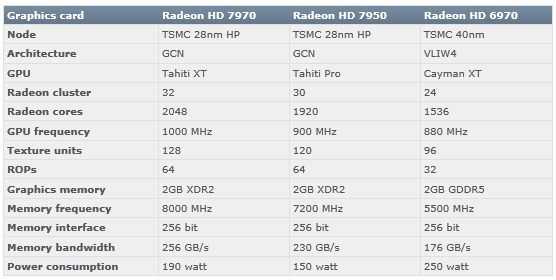
AMD's next-generation enthusiast graphics processor (GPU) is shaping up to be something more unique than expected. The GPU codenamed "Tahiti" is going to be bleeding-edge in terms of its feature-set. To begin with, there's talk that it will make use of PCI-Express Generation 3 (Gen 3) system bus, which will give it a mammoth 32 GB/s of system interface bandwidth. Next, Tahiti will use a number-crunching architecture that's a generation ahead of even the VLIW4 it released with Cayman. VLIW4 will make up for most of the HD 7000 series, but not the top-end Tahiti GPU, it will use what AMD is referring to as "CoreNext Architecture", which is expected to boost performance per square millimeter die area beyond even what VLIW4 manages.
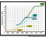
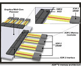
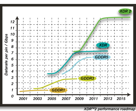
The most recent piece of information is bound to shock and awe. Tahiti, it appears, will use the XDR2 memory interface. XDR2 is an ultra-high bandwidth and power-efficient memory bus that's competitive with GDDR5, maintained by Rambus, which is claimed by it to be a generation ahead of GDDR5. It's not like XDR2 will be exotic to AIBs, the XDR architecture is used in game consoles where the high-bandwidth offsets low memory capacity by allowing quick streaming of texture data. Rambus licenses XDR memory chip manufacture to notable high-volume vendors. Nordic Hardware compiled data from various unreliable sources to sketch out what Radeon HD 7900 series could look like.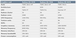
Source:
NordicHardware
The most recent piece of information is bound to shock and awe. Tahiti, it appears, will use the XDR2 memory interface. XDR2 is an ultra-high bandwidth and power-efficient memory bus that's competitive with GDDR5, maintained by Rambus, which is claimed by it to be a generation ahead of GDDR5. It's not like XDR2 will be exotic to AIBs, the XDR architecture is used in game consoles where the high-bandwidth offsets low memory capacity by allowing quick streaming of texture data. Rambus licenses XDR memory chip manufacture to notable high-volume vendors. Nordic Hardware compiled data from various unreliable sources to sketch out what Radeon HD 7900 series could look like.

54 Comments on Radeon HD 7900 Series to Use XDR2 Memory?
And yes, memory controller performance can have a large effect on the actual GPU. So a smaller IMC closer to the heart of the GPU core will improve performance as long as its design and implementation is good, but modern design allows for memory retraining, and a separate clock, and I believe ATI learned a lesson with the decoupling capacitors.
A faster memory does not automatically mean a reduction in silicon space, nor does it mean better thermals, etc. GPU designers make an election, for Cayman they decided to use faster memory and a big MC compared to Barts, twice as big in fact, so they could have gone with a 512 bit interface and only considering the chip it would have been better.
i.e
512 x 4000 = 256 GB/s
256 x 5000 = 160 GB/s
both requiring about the same size MC. They could have gone with
384 x 4000 = 192 GB/s
and it would have required less die space than Cypress' or Cayman's MC. They didn't follow that route because of more traces on the PCB.
So to sum it up, you said:All I'm saying is that that is not necessarily true, since a MC designed for very high frequencies can actually be much bigger than one designed for lower frequencies but is twice as wide. And sometimes it's not even that, sometimes a 50% wider MC can actually win in both metrics (pure performance + efficiency) as would have been the case if AMD had gone the 384 bit route.
IF it was fact and not rumors about AMD using XDR2 memory, it would make sense to think that's what AMD thought would help their architecture more, despite whatever downsides it could have. But they are rumors and they don't really make any sense at all. Not even Charlie D bites this and it would have made for a very "good" (CD style) article, where he could find a way to bash Nvidia for being behind and all. Instead he is bluntly denying this, which makes me suspect it's false.
What is the use of fast internal memory speed other than processing speed at device while you can't move the data faster between the devices.
2 cents
Never met a rambus product that was good.
(TBH: how are they still around? Patent lawsuits are a business structure?)