Tuesday, March 25th 2014

NVIDIA Launches World's First High-Speed GPU Interconnect
NVIDIA today announced that it plans to integrate a high-speed interconnect, called NVIDIA NVLink, into its future GPUs, enabling GPUs and CPUs to share data five to 12 times faster than they can today. This will eliminate a longstanding bottleneck and help pave the way for a new generation of exascale supercomputers that are 50-100 times faster than today's most powerful systems.
NVIDIA will add NVLink technology into its Pascal GPU architecture -- expected to be introduced in 2016 -- following this year's new NVIDIA Maxwell compute architecture. The new interconnect was co-developed with IBM, which is incorporating it in future versions of its POWER CPUs.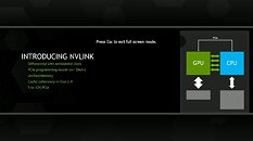
 "NVLink technology unlocks the GPU's full potential by dramatically improving data movement between the CPU and GPU, minimizing the time that the GPU has to wait for data to be processed," said Brian Kelleher, senior vice president of GPU Engineering at NVIDIA.
"NVLink enables fast data exchange between CPU and GPU, thereby improving data throughput through the computing system and overcoming a key bottleneck for accelerated computing today," said Bradley McCredie, vice president and IBM Fellow at IBM. "NVLink makes it easier for developers to modify high-performance and data analytics applications to take advantage of accelerated CPU-GPU systems. We think this technology represents another significant contribution to our OpenPOWER ecosystem."
With NVLink technology tightly coupling IBM POWER CPUs with NVIDIA Tesla GPUs, the POWER data center ecosystem will be able to fully leverage GPU acceleration for a diverse set of applications, such as high performance computing, data analytics and machine learning.
Advantages Over PCI Express 3.0
Today's GPUs are connected to x86-based CPUs through the PCI Express (PCIe) interface, which limits the GPU's ability to access the CPU memory system and is four- to five-times slower than typical CPU memory systems. PCIe is an even greater bottleneck between the GPU and IBM POWER CPUs, which have more bandwidth than x86 CPUs. As the NVLink interface will match the bandwidth of typical CPU memory systems, it will enable GPUs to access CPU memory at its full bandwidth.
This high-bandwidth interconnect will dramatically improve accelerated software application performance. Because of memory system differences -- GPUs have fast but small memories, and CPUs have large but slow memories -- accelerated computing applications typically move data from the network or disk storage to CPU memory, and then copy the data to GPU memory before it can be crunched by the GPU. With NVLink, the data moves between the CPU memory and GPU memory at much faster speeds, making GPU-accelerated applications run much faster.
Unified Memory Feature
Faster data movement, coupled with another feature known as Unified Memory, will simplify GPU accelerator programming. Unified Memory allows the programmer to treat the CPU and GPU memories as one block of memory. The programmer can operate on the data without worrying about whether it resides in the CPU's or GPU's memory.
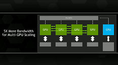
Although future NVIDIA GPUs will continue to support PCIe, NVLink technology will be used for connecting GPUs to NVLink-enabled CPUs as well as providing high-bandwidth connections directly between multiple GPUs. Also, despite its very high bandwidth, NVLink is substantially more energy efficient per bit transferred than PCIe.
NVIDIA has designed a module to house GPUs based on the Pascal architecture with NVLink. This new GPU module is one-third the size of the standard PCIe boards used for GPUs today. Connectors at the bottom of the Pascal module enable it to be plugged into the motherboard, improving system design and signal integrity.
NVLink high-speed interconnect will enable the tightly coupled systems that present a path to highly energy-efficient and scalable exascale supercomputers, running at 1,000 petaflops (1 x 10¹⁸ floating point operations per second), or 50 to 100 times faster than today's fastest systems.
NVIDIA will add NVLink technology into its Pascal GPU architecture -- expected to be introduced in 2016 -- following this year's new NVIDIA Maxwell compute architecture. The new interconnect was co-developed with IBM, which is incorporating it in future versions of its POWER CPUs.


"NVLink enables fast data exchange between CPU and GPU, thereby improving data throughput through the computing system and overcoming a key bottleneck for accelerated computing today," said Bradley McCredie, vice president and IBM Fellow at IBM. "NVLink makes it easier for developers to modify high-performance and data analytics applications to take advantage of accelerated CPU-GPU systems. We think this technology represents another significant contribution to our OpenPOWER ecosystem."
With NVLink technology tightly coupling IBM POWER CPUs with NVIDIA Tesla GPUs, the POWER data center ecosystem will be able to fully leverage GPU acceleration for a diverse set of applications, such as high performance computing, data analytics and machine learning.
Advantages Over PCI Express 3.0
Today's GPUs are connected to x86-based CPUs through the PCI Express (PCIe) interface, which limits the GPU's ability to access the CPU memory system and is four- to five-times slower than typical CPU memory systems. PCIe is an even greater bottleneck between the GPU and IBM POWER CPUs, which have more bandwidth than x86 CPUs. As the NVLink interface will match the bandwidth of typical CPU memory systems, it will enable GPUs to access CPU memory at its full bandwidth.
This high-bandwidth interconnect will dramatically improve accelerated software application performance. Because of memory system differences -- GPUs have fast but small memories, and CPUs have large but slow memories -- accelerated computing applications typically move data from the network or disk storage to CPU memory, and then copy the data to GPU memory before it can be crunched by the GPU. With NVLink, the data moves between the CPU memory and GPU memory at much faster speeds, making GPU-accelerated applications run much faster.
Unified Memory Feature
Faster data movement, coupled with another feature known as Unified Memory, will simplify GPU accelerator programming. Unified Memory allows the programmer to treat the CPU and GPU memories as one block of memory. The programmer can operate on the data without worrying about whether it resides in the CPU's or GPU's memory.
Although future NVIDIA GPUs will continue to support PCIe, NVLink technology will be used for connecting GPUs to NVLink-enabled CPUs as well as providing high-bandwidth connections directly between multiple GPUs. Also, despite its very high bandwidth, NVLink is substantially more energy efficient per bit transferred than PCIe.
NVIDIA has designed a module to house GPUs based on the Pascal architecture with NVLink. This new GPU module is one-third the size of the standard PCIe boards used for GPUs today. Connectors at the bottom of the Pascal module enable it to be plugged into the motherboard, improving system design and signal integrity.
NVLink high-speed interconnect will enable the tightly coupled systems that present a path to highly energy-efficient and scalable exascale supercomputers, running at 1,000 petaflops (1 x 10¹⁸ floating point operations per second), or 50 to 100 times faster than today's fastest systems.
22 Comments on NVIDIA Launches World's First High-Speed GPU Interconnect
;)
As is the norm, AMD creates the idea, and Nvidia brings a useable form to the masses. Tech partnerships at it's best, really.
They say it's because they need access to CPU memory and that GPU memory is "small", but I think again we've seen the opposite trend. Plenty of enthusiast computers have 16GB of main memory but have easily 3-4GB of VRAM per card. Is it just that a lot of main memory isn't used in gaming, and you can just hoard textures in there if you had more bandwidth?
A limitation in gaming? Yes AND No. AMD Multi-GPU stutter problems are due to PCIe limitations.
If you watched Nvidia's promo...they easily pointed out that in order to provide what is needed to make a real jump in graphics, requires 1000's of bits of memory interconnect...compared to the 384 we have today. Being able to feed that memory, as well as other GPUs, is not possible over PCIe...hence NV-LINK.
I will be glad to buy a mobo that has both NVLINK and PCIe. Especially tired of seeing Intel's lack of PCIe 4, DDR4, new technology interfaces, etc on their Z97 and X99 platforms.
*EDIT, just noticed I had put in 2026, instead of 2016. :oops:
Although, the mention of IBM POWERPC chips...kinda...well...removes my excitement. :roll:
Looking at the physical sample NV showed today, it looks a lot like a module for the new Apple MAC PRO trashcan-PC.
If that's Nvidia's choice to stay relevant to the marketplace...to work with Apple...well...
The Titan-Z is already outdated, wait for the Titan-Z2 with 12GB of unified memory ;)
Oh wait, that's exactly the scenario hinted at in the presentation...:p and shown in the slides.
Is it just me or does it seem like someone threw the PR team there out a window and they are trying to make enough PR slides to land on.