Thursday, January 15th 2015

Samsung Starts Mass Producing Industry's First 8 Gb GDDR5 Memory
Samsung Electronics Co., Ltd., the world leader in advanced memory technology, announced today that it has begun mass producing the industry's first 8 gigabit (Gb) GDDR5 DRAM, based on the company's leading-edge 20-nanometer (nm) process technology. GDDR5 is the most widely used discrete graphics memory in the world.
Designed for use in graphics cards for PCs and supercomputing applications, and on-board graphics memory for game consoles and notebook PCs, discrete graphics DRAM provides an extensive amount of bandwidth to process large high quality graphically-oriented data streams. With the rising popularity of 3-D games and UHD video content soon to be widespread, the need for high-performance, high-bandwidth graphics memory has begun to rapidly increase.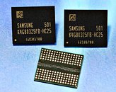 "We expect that our 8Gb GDDR5 will provide original equipment manufacturers (OEMs) with the best graphics memory solution available for game consoles as well as general use notebook PCs," said Joo Sun Choi, Executive Vice president of Memory Sales and Marketing at Samsung Electronics. "By expanding our production of 20nm-based DRAM products including the new GDDR5, we will meet increasing global customer demand and take the lead in accelerating the growth of the premium memory market."
Samsung's new GDDR5 DRAM offers outstanding bandwidth. Combining only eight of the new 8Gb chips will achieve the same density as the 8 gigabytes (GB) needed in the latest game consoles.
The memory operates with an I/O data rate of 8 gigabits per second (Gbps) per pin, which is more than four times faster than the DDR3 DRAM widely used in notebook PCs today, and each chip can process data at 32-bit I/O rate. Two GB of graphics memory can be created with just two of the new chips, which together can process up to 64GB of graphical images per second. That equates to processing approximately 12 full-HD DVDs (5GB equivalent) in a second.
With this new 20nm 8Gb GDDR5, Samsung has completed its line-up of 8Gb DRAM solutions based on its leading-edge 20nm process technology, covering the server, PC, mobile and graphics memory markets. The world's largest memory manufacturer will keep expanding the production volumes of its 20nm DRAM products at a variety of densities including 4Gb, 6Gb, 8Gb and higher densities to solidify its leading position in high-end IT market segments as well as more value-driven markets.
Designed for use in graphics cards for PCs and supercomputing applications, and on-board graphics memory for game consoles and notebook PCs, discrete graphics DRAM provides an extensive amount of bandwidth to process large high quality graphically-oriented data streams. With the rising popularity of 3-D games and UHD video content soon to be widespread, the need for high-performance, high-bandwidth graphics memory has begun to rapidly increase.

Samsung's new GDDR5 DRAM offers outstanding bandwidth. Combining only eight of the new 8Gb chips will achieve the same density as the 8 gigabytes (GB) needed in the latest game consoles.
The memory operates with an I/O data rate of 8 gigabits per second (Gbps) per pin, which is more than four times faster than the DDR3 DRAM widely used in notebook PCs today, and each chip can process data at 32-bit I/O rate. Two GB of graphics memory can be created with just two of the new chips, which together can process up to 64GB of graphical images per second. That equates to processing approximately 12 full-HD DVDs (5GB equivalent) in a second.
With this new 20nm 8Gb GDDR5, Samsung has completed its line-up of 8Gb DRAM solutions based on its leading-edge 20nm process technology, covering the server, PC, mobile and graphics memory markets. The world's largest memory manufacturer will keep expanding the production volumes of its 20nm DRAM products at a variety of densities including 4Gb, 6Gb, 8Gb and higher densities to solidify its leading position in high-end IT market segments as well as more value-driven markets.
15 Comments on Samsung Starts Mass Producing Industry's First 8 Gb GDDR5 Memory
It takes very little to switch manifacture, capacity or type
Another interesting part about 8Gbps is practicality of use. We've seen that with 7gbps it really approaches the feasibility of memory controller size and pad space, which is more and more impractical as transistor sizes shrink and demand more bandwidth from less chip area (a chip needs to be pretty big, and memory controller extraordinarily/impractically large to use 8gbps...mem controller has to increase exponentially over ~5.5gbps). While it makes sense if combining a design that uses supplemental on-die cache to use less and faster controllers with perhaps faster (and vicariously less) memory if it fits a well thought-out overall design (per market), if we're strictly talking about the most efficient way of getting the most bandwidth from off-die sources, I would think it would make a lot more sense to increase the bus width (slow and fat) given it would be just, if not more, practical (ex: 384-bit 5-6gbps vs 256-bit 7-8gbps). AMD has pretty much always chosen this route, and I generally agree with it. In many cases making a chip *just* big-enough for a slower fat bus versus a faster, skinnier one has paid dividends. That includes AMD's long-history of successful ~200mm2 chips (rv670, Pitcairn, etc)...it's also very much the case in Tahiti and especially Hawaii.
That said...I'm kinda/sorta curious if Full Tonga will use something like this (granted it would need to come from Hynix, most likely...but they usually stay roughly in parody). I know it's long been said that chip contains a 384-bit bus...but if it didn't, that is the type of die size we'd be talking where 256-bit 8gbps *could* work, and perhaps a 2/4/8GB design may make more sense than 3/6/12. Another is GM204. That is how large a 256-bit chip needs to be for 8gbps to make make any kind of sense (granted the higher density is welcome)....almost impractically large. I smell '975' and '985' incoming....8gbps/8GB sounds like as good a reason as any to refresh GM204 (just like GK104 before it) as a more mid-range product (but with value-add over the older products) when big Maxwell launches to the masses.
Out of curiosity, has anyone seen the voltage listed anywhere, and/or how it compares to slower chips on the same process (which must exist)? I'm curious, for instance, if this is 1.6v (as was originally planned but never shipped on the older process), and if we've gotten a better power envelope for 5-6gbps (1.2v?).
For example, the current standard for GDDR5 is 7Gbps (7 GHz quad pumped, or "effective"), so for arguments sake a comparison of a 384-bit/ 7GHz memory part:
GTX 780Ti : 7Gbps / 8 (bits per byte) = 0.875 GB/sec * 64 I/O pins per controller = 56GB/sec * 6 memory controllers ( 64*6 = 384-bit) = 336GB/sectotal bandwidth
The same parameters used with 8Gbps GDDR5
GTX Titan-X (?): 8Gbps / 8 (bits per byte) = 1 GB/sec * 64 I/O pins per controller = 64GB/sec * 6 memory controllers ( 64*6 = 384-bit) = 384GB/sec total bandwidth ( add 33% to this (510GB/sec) to take into account colour compression if you're looking at a direct comparison with the Kepler architecture)