Thursday, November 5th 2015

AMD "Fiji" GPU Die-shot Revealed by Chipworks
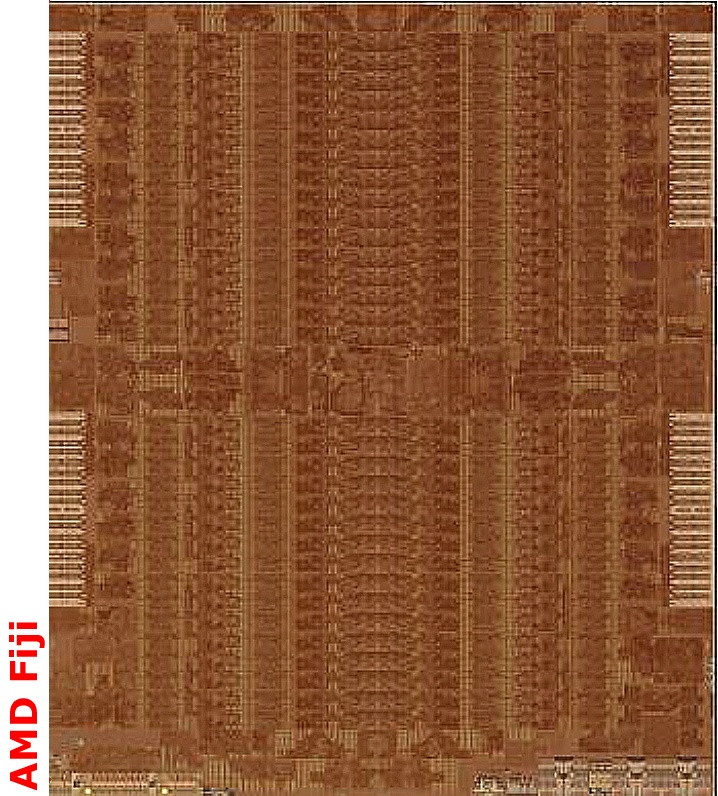
VLSI technical publication Chipworks posted the first clear die-shot of AMD's "Fiji" silicon, revealing intricate details of the most technically advanced GPU. What makes Fiji the most advanced graphics chip is its silicon interposer and stacked HBM chips making up a multi-chip module. It's the die in the center of all that, which went under Chipworks' microscope.
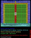
The die-shot reveals a component layout that's more or less an upscale of "Tonga." Some of the components, such as the front-end appear to be entirely identical to "Tahiti" or "Tonga." The shot reveals the 64 GCN compute units arranged in four rows, on either side of the central portion with the dispatch and primitive setup pipelines. The pad-area of the on-die memory controllers appear to be less than the large memory I/O pads that made up the 384-bit interface of "Tahiti." The first picture below is the die-shot of "Fiji," followed by a color-coded die-shot of "Tahiti."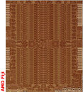
Sources:
3DCenter.org, ChipWorks
The die-shot reveals a component layout that's more or less an upscale of "Tonga." Some of the components, such as the front-end appear to be entirely identical to "Tahiti" or "Tonga." The shot reveals the 64 GCN compute units arranged in four rows, on either side of the central portion with the dispatch and primitive setup pipelines. The pad-area of the on-die memory controllers appear to be less than the large memory I/O pads that made up the 384-bit interface of "Tahiti." The first picture below is the die-shot of "Fiji," followed by a color-coded die-shot of "Tahiti."

3 Comments on AMD "Fiji" GPU Die-shot Revealed by Chipworks