Thursday, May 5th 2016

AMD "Summit Ridge" Silicon Reserved for 8-core CPUs Initially
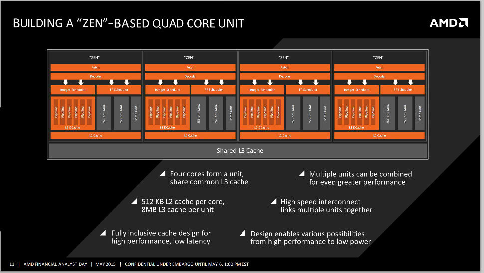
Sources tell Bits'n'Chips that AMD could use a common 8-core CPU die based on its upcoming "Zen" architecture over multiple CPU SKUs, at least initially. AMD will have two distinct kinds of processors, those with integrated graphics (APUs) based on the "Bristol Ridge" silicon, and those without integrated graphics (CPUs), based on the "Summit Ridge" silicon. Since products based on both the dies will use a common socket on the desktop (socket AM4), consumers looking for 2-4 CPU cores will be presented with APU options, while those looking for more powerful CPU solutions will be made to choose 8-core CPUs based on the "Summit Ridge" silicon.
Source:
BitsnChips.it
76 Comments on AMD "Summit Ridge" Silicon Reserved for 8-core CPUs Initially
So to answer what you are saying there are multiple things that have to happen to make any of what you said even possible. First the new manufacturing process has to actually lower voltage, otherwise TDP will remain the same. The architecture has to actually scale higher (k8 is a good example of peaking a design). Not to mention what is you definition of more power? PD840EE was faster than the PD940, yet the latter was based off of a die shrink. I can overclock a PD805 faster than most of the 9x0 series duals, yet it is an older bigger die. A lot of these designs have a max clockspeed regardless of die size; netburst, K8, K10, C2D's all of these litho's had a max speed that shrinking the die didn't change. They offered the same performance as their predecessor if nothing else was changed (most gains you saw were architecture and cache size increases).Again the die shrink will change nothing in physical performance. All it allows is more transistors in the same surface area, if the manufacturer chooses to redesign and add more transistors (change the architecture) at that point you will see a performance change. You keep adding multiple changes and calling it all a die shrink. Not all die shrinks add jack shit if you will. In fact most inter-design die shrinks add next to no performance.