Monday, June 17th 2019

Intel "Ice Lake" IPC Best-Case a Massive 40% Uplift Over "Skylake," 18% on Average

Intel late-May made its first major disclosure of the per-core CPU performance gains achieved with its "Ice Lake" processor that packs "Sunny Cove" CPU cores. Averaged across a spectrum of benchmarks, Intel claims a best-case scenario IPC (instructions per clock) uplift of a massive 40 percent over "Skylake," and a mean uplift of 18 percent. The worst-case scenario sees its performance negligibly below that of "Skylake." Intel's IPC figures are derived entirely across synthetic benchmarks, which include SPEC 2016, SPEC 2017, SYSMark 2014 SE, WebXprt, and CineBench R15. The comparison to "Skylake" is relevant because Intel has been using essentially the same CPU core in the succeeding three generations that include "Kaby Lake" and "Coffee Lake."

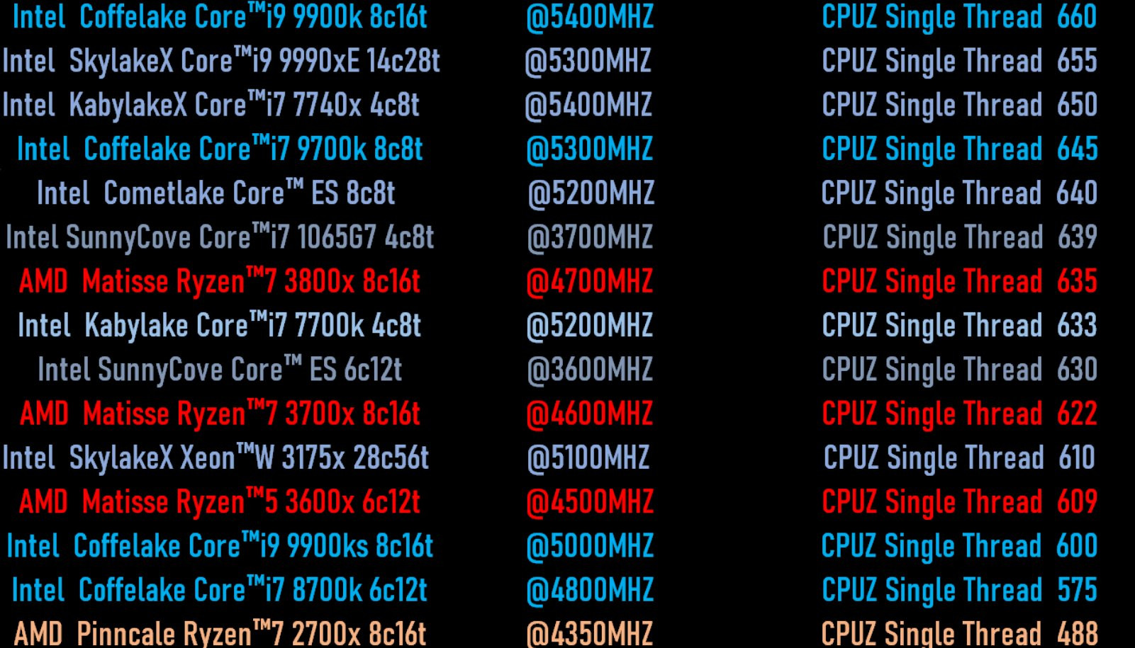
A Chinese tech-forum member with access to an "Ice Lake" 6-core/12-thread sample put the chip through the CPU-Z internal benchmark (test module version 17.01). At a clock-speed of 3.60 GHz, the "Ice Lake" chip allegedly achieved a single-core score of 635 points. To put this number into perspective, a Ryzen 7 3800X "Matisse" supposedly needs to run at 4.70 GHz to match this score, and a Core i7-7700K "Kaby Lake" needs to run at 5.20 GHz. Desktop "Ice Lake" processors are unlikely to launch in 2019. The first "Ice Lake" processors are 4-core/8-thread chips designed for ultraportable notebook platforms, which come out in Q4-2019, and desktop "Ice Lake" parts are expected only in 2020.
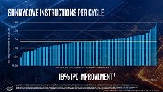
Source: WCCFTech
Add your own comment

153 Comments on Intel "Ice Lake" IPC Best-Case a Massive 40% Uplift Over "Skylake," 18% on Average

#76
Vya Domus
OSdevrNo they don't. Intel's tick-tock scheme alternated between new architecture and new process.
A monolithic 16 core from AMD would fall in the 250 mm^2 region on 7nm. An Intel equivalent would need 400+ on 14nm, they needed 10nm to make competitive products. Tick-tock worked up until now because they always had the leading node, now they don't.

Developing an architecture without a new node isn't ideal.
Posted on Reply
#77
OSdevr
Vya DomusA monolithic 16 core from AMD would fall in the 250 mm^2 region on 7nm. An Intel equivalent would need 400+ on 14nm, they needed 10nm to make competitive products. Tick-tock worked up until now because they always had the leading node, now they don't.

Developing an architecture without a new node isn't ideal.
You're talking about frequency and number of cores not the IPC of each. IPC increases don't usually require huge increases in die size (though cache increases can), hyper-threading only increased the Pentium 4's die by 5%.

Obviously it'd be nice if each new architecture had a new node to go with it, but it's hardly necessary.
Posted on Reply
#78
Space Lynx
Astronaut
XzibitIntel has other plans. At least thats what it told its investors this year.


Intel will be using Arizona and Ireland for 7nm. Expansion at those fabs is expected to be completed late 2021 for Arizona, Ireland est sometime in 2022.

looks like I am rolling 12 core 3900x until 2022/2023 then.
TheLostSwedeI have no idea, but your reading comprehension clearly needs to improve.
The first image is from an Intel presentation, using only synthetic benchmarks, whereas when AMD used them during their presentation at Computex, Intel went out and said that from now, we should only use real world benchmarks. Yet Intel clearly seems more than happy to use synthetic benchmarks when it suits them. As such, this is irrelevant even by Intel's "new" standards, no?
AMD uses synthetic too, this is just part of the industry... don't forget Navi unviel, they only showed Strange Brigade and nothing else... sad... this is just part of business marketing... get over it?
Posted on Reply
#79
RichF
AquinusI need to see it to believe it. Let me guess; This is before all of the security vulnerability mitigations compared to a CPU with them enabled? :laugh:
Apparently we're supposed to believe that all of the vulnerabilities and regressions from mitigations will be fixed. I'll believe it when I see it.

The reasoning goes that Intel has plenty of time to fix the plethora of vulnerabilities and rectify the regressions. At the pace new Intel-only vulnerabilities have been popping up I don't think it's that outlandish to expect new ones in relatively short order either.

One might quip that Intel's best hope is to find devastating vulnerabilities in AMD's CPUs, along the lines of having to completely disable hyperthreading. :rolleyes:

It's a bit mind-boggling that so many seem to so blithely accept such massive defects in Intel's CPUs. The mentality is "just go and buy another one", as if there is unlimited money. Planned obsolescence at its most inglorious?
Posted on Reply
#80
TheLostSwede
News Editor
lynx29AMD uses synthetic too, this is just part of the industry... don't forget Navi unviel, they only showed Strange Brigade and nothing else... sad... this is just part of business marketing... get over it?
I never said they didn't, my point was that Intel now says we should only use real world benchmarks. How do you benchmark steam or VLC?
Posted on Reply
#81
ratirt
TheLostSwedeI never said they didn't, my point was that Intel now says we should only use real world benchmarks. How do you benchmark steam or VLC?
I'd bet Intel would come up with an idea of how to do it and of course Intel's CPUs would be the fastest.
Posted on Reply
#82
londiste
Vya DomusA monolithic 16 core from AMD would fall in the 250 mm^2 region on 7nm. An Intel equivalent would need 400+ on 14nm, they needed 10nm to make competitive products.
Considering 8-core die in 9900K is 175mm^2 with iGPU, Intel could do a 16-core at around 350mm^2 and probably less than that.
I am willing to bet AMD can do a monolithic 16 core at around 200mm^2 on 7nm. 8-core chiplets are 75-80mm^2 and 12/14nm IO Die is 120mm^2. There are a lot of extra things in IO Die that are not strictly required.

We will probably get a good idea about what AMD can do with 7nm in terms of cores and die size when APUs come out. Intel is still betting on 4-core mobile CPUs (which is probably not a bad idea) and AMDs current response is 12nm Zen+ APUs but 7nm APUs should replace these within a years time.
Posted on Reply
#83
Vya Domus
londisteIntel could do a 16-core at around 350mm^2 and probably less than that.
Not with Sunny Cove and whatever next generation integrated graphics they made.
Posted on Reply
#84
londiste
Integrated graphics wouldn't play much of a part in 16-core CPU. 64 EU or even 48 EU iGPUs would not make much sense. A minimal 8 EU or lack of iGPU would be OK.
You are right about Sunny Cove though, doubled caches will increase the size notably.
Posted on Reply
#85
InVasMani
londisteConsidering 8-core die in 9900K is 175mm^2 with iGPU, Intel could do a 16-core at around 350mm^2 and probably less than that.
I am willing to bet AMD can do a monolithic 16 core at around 200mm^2 on 7nm. 8-core chiplets are 75-80mm^2 and 12/14nm IO Die is 120mm^2. There are a lot of extra things in IO Die that are not strictly required.

We will probably get a good idea about what AMD can do with 7nm in terms of cores and die size when APUs come out. Intel is still betting on 4-core mobile CPUs (which is probably not a bad idea) and AMDs current response is 12nm Zen+ APUs but 7nm APUs should replace these within a years time.
I have to wonder if AMD might integrate a dual/quad core CPU/APU into the I/O Die with a node shrink and split in half some of the I/O die logic that it can serve and use more than one I/O die. That could be a good way of getting around some of the issues surrounding system interrupts under heavy stress loads. If one I/O die is heavily loaded it wouldn't bog down the the other. So if one I/O die with some storage devices/USB devices is heavily strained the I/O die could be functioning at top speed and load balance the overall system more effectively. I'm just speculating on a possibility of a direction it might move toward with a bit more revision.

I tend to think at 5nm we'll see a pair CPU core/thread die's and pair of I/O die's with about half the logic split between the two which will bring down the temperatures of them a bit. The chipset could be a multi chip solution as well might as well if made sense for the CPU probably does for the chipset as well.
Posted on Reply
#86
quadibloc
AMD doubled the vector floating-point muscle of the upcoming generation of Ryzen chips. To me, that's the biggest news about them, and likely the main reason they can be considered to have caught up with Intel.
But Intel was about to double theirs as well, putting AMD back where it was. Although they have some 10nm parts in volume production, the desktop chips that were going to bring AVX-512 support to the mainstream aren't here yet.
So, while Intel and AMD have made comparable IPC improvements, it seems to me that AMD has not done everything it should have done to obtain a solid lead over Intel, and their current lead is simply a result of Intel having some unexpected further delays with its 10nm lineup. So, while I still feel pretty excited over the new Ryzens, I take a somewhat cautious view.
Posted on Reply
#87
TheMadDutchDude
I’m calling it now, if it hasn’t been called already: they used XTU to show performance gain.
Posted on Reply
#88
BorgOvermind
TheLostSwedeHang on a second there, didn't Intel say they only wanted to use real world benchmarks from now on?
That means this is against their own policy and clearly irrelevant, no?
Only when it favors them, of course.
Posted on Reply
#89
Litzner
This feels like Intel releasing some BS numbers about a product on a process Intel can't do right before Ryzen comes out just to try to get people not to switch teams.
Posted on Reply
#90
InVasMani
Real world I don't always single task, I tend to care about safety and security, windows updates when it chooses, steam downloads in the background, people download in the background, people install stuff in the background, and in the only time I play games in 1080p is never or when the game runs as badly as RTX and I want to prematurely ||||||||||||| over how much better old graphics could have looked with better hardware or with wooden screws added.
Posted on Reply
#91
GoldenX
If this is true, why didn't Intel do it sooner? 10nm is not an IPC changer, their design is.
We were recieving 5% IPC increases or even less for 10 years and suddenly, boom, 18%, just when AMD seems to get the lead.
Posted on Reply
#92
efikkan
GoldenXIf this is true, why didn't Intel do it sooner? 10nm is not an IPC changer, their design is.

We were recieving 5% IPC increases or even less for 10 years and suddenly, boom, 18%, just when AMD seems to get the lead.
We know why; Ice Lake has been ready for nearly two years, just waiting for a suitable node.
AMD has nothing to do with it.
Posted on Reply
#93
HwGeek
Intel will put big effort in the HPC GPU area since for each Xeon they can sell more then 4 HPC GPUs that cost upto $20K each, it's a big money.
Posted on Reply
#94
trparky
quadiblocAVX-512
The question of course is... Are there any applications in play that use AVX-512 extensions outside of custom scientific applications?

I've done some research into this and it seems that most programs in use by regular people (programs like Firefox, Google Chrome, 7-ZIP, Photoshop, etc.) are using AVX2 (that's AVX-256) which is what is now supported by Zen 2 or Ryzen 3000. AVX-512 may be the newest kind of AVX instructions but it seems that it's still only used in limited and very custom workloads, not in general use.

And besides, for most Intel chips in use today whenever they start executing AVX-256 bit instructions they tend to clock down via the AVX-offset generally because to execute AVX instructions it requires more power thus more heat and thus they can't run at their regular clock speed. AMD's new Zen 2 architecture appears (or at least what AMD has said) doesn't require some kind of AVX-offset while executing AVX-256 bit instructions which the way I see it is that the new Ryzen 3000 series of chips won't downclock while executing AVX-256 bit instructions as their Intel counterparts do thus we'll see better performance from AMD chips than Intel chips while performing AVX-256 bit workloads.
Posted on Reply
#95
efikkan
trparkyAVX-512 may be the newest kind of AVX instructions but it seems that it's still only used in limited and very custom workloads, not in general use.
Yes, so far.
But you got to start somewhere, hardware support usually have to come first.
Posted on Reply
#96
Vya Domus
trparkyThe question of course is... Are there any applications in play that use AVX-512 extensions outside of custom scientific applications?
Nope. Whats worse is that AVX 512 workloads don't scale as well as AVX1/2 which in turn scaled worse than SSE. Increasing AVX2 throughput is more useful as far as I am concerned.
Posted on Reply
#97
yeeeeman
What about this benchmark? www.notebookcheck.net/Intel-s-Ice-Lake-i7-1065G7-CPU-briefly-pops-up-on-PassMark-and-outstrips-AMD-s-new-Picasso-Ryzen-7-3750H-APU.424636.0.html
This is Passmark. Single thread score at ~4.8 Ghz (short test, might actually run at 4.8Ghz) of 8665U is 2400 points. 1065G7 gets 2625 points, at 3.9 Ghz. If we get the 1065G7 to 4.8 Ghz, we get 3200 points. That would translate into 34% higher IPC. Any thoughts? I was also skeptical about the 40% mentioned in this stupid forum picture, but passmark looks a bit more legit to me.
Posted on Reply
#98
londiste
yeeeemanWhat about this benchmark? www.notebookcheck.net/Intel-s-Ice-Lake-i7-1065G7-CPU-briefly-pops-up-on-PassMark-and-outstrips-AMD-s-new-Picasso-Ryzen-7-3750H-APU.424636.0.html
This is Passmark. Single thread score at ~4.8 Ghz (short test, might actually run at 4.8Ghz) of 8665U is 2400 points. 1065G7 gets 2625 points, at 3.9 Ghz. If we get the 1065G7 to 4.8 Ghz, we get 3200 points. That would translate into 34% higher IPC. Any thoughts? I was also skeptical about the 40% mentioned in this stupid forum picture, but passmark looks a bit more legit to me.
Early hardware and incorrectly reported clock speeds? Intel implementing something new in terms of frequency boost that goes beyond specced boost clock?
That is a 35% difference, sounds very unrealistic.
Posted on Reply
#99
efikkan
londisteEarly hardware and incorrectly reported clock speeds? Intel implementing something new in terms of frequency boost that goes beyond specced boost clock?

That is a 35% difference, sounds very unrealistic.
It's very common that clockspeeds for new and future products are inaccurate.
While Intel have become more aggressive in boosting over the years, AMD took it to a new level with XFR's extra ~200 MHz for burst speed. This sort of stuff can't be accurately measured. This super aggressive boosting is more about manipulating benchmark scores than offering actual improvements, but (unfortunately) I expect Intel to push it further too.
Posted on Reply
#100
trparky
Boost speeds are nice and all but only if the boost speeds last longer than a second or two. What many of us need is sustained and consistent performance and not a couple of short boosts in speed when the time is right and the chip is sufficiently cool enough to be able to do it.

And then we have the benchmarks that yeah, they show amazing numbers but how do those numbers translate into real-world performance? It's great if you're the benchmark king but at the end of the day what really matters is how much work you can get done in a certain time frame. We've even seen it with SSDs, sure the sustained throughput numbers look great but do they necessarily translate to faster loading software? Nope, 4K random reads are still semi the same over the last few years.
Posted on Reply
Add your own comment
May 7th, 2024 08:17 EDT change timezone

New Forum Posts

Popular Reviews

Controversial News Posts