Report an Error


NVIDIA GeForce GTX 950
- Graphics Processor
- GM206
- Cores
- 768
- TMUs
- 48
- ROPs
- 32
- Memory Size
- 2 GB
- Memory Type
- GDDR5
- Bus Width
- 128 bit


GPU
I/O

Top
Recommended Gaming Resolutions:
- 1600x900
- 1920x1080
- 2560x1440
The GeForce GTX 950 was a mid-range graphics card by NVIDIA, launched on August 20th, 2015. Built on the 28 nm process, and based on the GM206 graphics processor, in its GM206-250-A1 variant, the card supports DirectX 12. This ensures that all modern games will run on GeForce GTX 950. The GM206 graphics processor is an average sized chip with a die area of 228 mm² and 2,940 million transistors. Unlike the fully unlocked GeForce GTX 960, which uses the same GPU but has all 1024 shaders enabled, NVIDIA has disabled some shading units on the GeForce GTX 950 to reach the product's target shader count. It features 768 shading units, 48 texture mapping units, and 32 ROPs. NVIDIA has paired 2,048 MB GDDR5 memory with the GeForce GTX 950, which are connected using a 128-bit memory interface. The GPU is operating at a frequency of 1024 MHz, which can be boosted up to 1188 MHz, memory is running at 1653 MHz (6.6 Gbps effective).
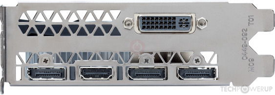
Being a dual-slot card, the NVIDIA GeForce GTX 950 draws power from 1x 6-pin power connector, with power draw rated at 90 W maximum. Display outputs include: 1x DVI, 1x HDMI 2.0, 3x DisplayPort 1.2. GeForce GTX 950 is connected to the rest of the system using a PCI-Express 3.0 x16 interface. The card measures 202 mm in length, and features a dual-slot cooling solution. Its price at launch was 159 US Dollars.
Being a dual-slot card, the NVIDIA GeForce GTX 950 draws power from 1x 6-pin power connector, with power draw rated at 90 W maximum. Display outputs include: 1x DVI, 1x HDMI 2.0, 3x DisplayPort 1.2. GeForce GTX 950 is connected to the rest of the system using a PCI-Express 3.0 x16 interface. The card measures 202 mm in length, and features a dual-slot cooling solution. Its price at launch was 159 US Dollars.
Graphics Processor
- GPU Name
- GM206
- GPU Variant
- GM206-250-A1
- Architecture
- Maxwell 2.0
- Foundry
- TSMC
- Process Size
- 28 nm
- Transistors
- 2,940 million
- Density
- 12.9M / mm²
- Die Size
- 228 mm²
- Chip Package
- BGA-1428
Graphics Card
- Release Date
- Aug 20th, 2015
- Generation
- GeForce 900
- Predecessor
- GeForce 700
- Successor
- GeForce 10
- Production
- End-of-life
- Launch Price
- 159 USD
- Bus Interface
- PCIe 3.0 x16
- Reviews
- 76 in our database
Relative Performance
Based on TPU review data: "Performance Summary" at 1920x1080, 4K for 2080 Ti and faster.
Clock Speeds
- Base Clock
- 1024 MHz
- Boost Clock
- 1188 MHz
- Memory Clock
-
1653 MHz
6.6 Gbps effective
Memory
- Memory Size
- 2 GB
- Memory Type
- GDDR5
- Memory Bus
- 128 bit
- Bandwidth
- 105.8 GB/s
Render Config
- Shading Units
- 768
- TMUs
- 48
- ROPs
- 32
- SMM Count
- 6
- L1 Cache
- 48 KB (per SMM)
- L2 Cache
- 1024 KB
Theoretical Performance
- Pixel Rate
- 38.02 GPixel/s
- Texture Rate
- 57.02 GTexel/s
- FP32 (float)
- 1.825 TFLOPS
- FP64 (double)
- 57.02 GFLOPS (1:32)
Board Design
- Slot Width
- Dual-slot
- Length
- 202 mm
8 inches
- TDP
- 90 W
- Suggested PSU
- 250 W
- Outputs
- 1x DVI
1x HDMI 2.0
3x DisplayPort 1.2
- Power Connectors
- 1x 6-pin
Graphics Features
- DirectX
- 12 (12_1)
- OpenGL
- 4.6
- OpenCL
- 3.0
- Vulkan
- 1.3
- CUDA
- 5.2
- Shader Model
- 6.7
GM206 GPU Notes
| NVENC: 5th Gen NVDEC: 2nd Gen PureVideo HD: VP7 VDPAU: Feature Set F |
Retail boards based on this design (50)
| Name | GPU Clock | Boost Clock | Memory Clock | Other Changes |
|---|---|---|---|---|
| 1140 MHz | 1329 MHz | 1653 MHz | 221 mm/8.7 inches, 2x DVI 1x HDMI 1x DisplayPort | |
| 1026 MHz | 1190 MHz | 1653 MHz | 211 mm/8.3 inches, 1x DVI 1x HDMI 1x DisplayPort | |
| 1026 MHz | 1190 MHz | 1653 MHz | 211 mm/8.3 inches, 1x DVI 1x HDMI 1x DisplayPort | |
| 1026 MHz | 1190 MHz | 1653 MHz | 173 mm/6.8 inches, 1x DVI 1x HDMI 1x DisplayPort | |
| 1076 MHz | 1253 MHz | 1653 MHz | 211 mm/8.3 inches, 1x DVI 1x HDMI 1x DisplayPort | |
| 1026 MHz | 1190 MHz | 1653 MHz | 221 mm/8.7 inches, 2x DVI 1x HDMI 1x DisplayPort | |
| 1140 MHz | 1329 MHz | 1653 MHz | 221 mm/8.7 inches, 2x DVI 1x HDMI 1x DisplayPort | |
| 1140 MHz | 1329 MHz | 1653 MHz | 2x DVI 1x HDMI 1x DisplayPort | |
| 1140 MHz | 1329 MHz | 1653 MHz | 2x DVI 1x HDMI 1x DisplayPort | |
| 1140 MHz | 1329 MHz | 1653 MHz | 2x DVI 1x HDMI 1x DisplayPort | |
| 1216 MHz | 1418 MHz | 1653 MHz | 2x DVI 1x HDMI 1x DisplayPort | |
| 1178 MHz | 1367 MHz | 1750 MHz | 2x DVI 1x HDMI 1x DisplayPort | |
| 1102 MHz | 1279 MHz | 1653 MHz | ||
| 1026 MHz | 1190 MHz | 1653 MHz | 173 mm/6.8 inches, 1x DVI 1x HDMI 1x DisplayPort | |
| 1026 MHz | 1190 MHz | 1653 MHz | 173 mm/6.8 inches, 2x DVI 1x HDMI 1x DisplayPort | |
| 1203 MHz | 1405 MHz | 1653 MHz | 257 mm/10.1 inches | |
| 1076 MHz | 1253 MHz | 1653 MHz | 173 mm/6.8 inches, 1x DVI 1x HDMI 1x DisplayPort | |
| 1076 MHz | 1253 MHz | 1653 MHz | 173 mm/6.8 inches, 2x DVI 1x HDMI 1x DisplayPort | |
| 1190 MHz | 1393 MHz | 1653 MHz | 257 mm/10.1 inches | |
| 1190 MHz | 1393 MHz | 1653 MHz | 257 mm/10.1 inches | |
| 1152 MHz | 1342 MHz | 1653 MHz | 173 mm/6.8 inches | |
| 1165 MHz | 1355 MHz | 1653 MHz | 257 mm/10.1 inches | |
| 1024 MHz | 1188 MHz | 1653 MHz | ||
| 1024 MHz | 1188 MHz | 1653 MHz | 222 mm/8.7 inches, 2x DVI 1x HDMI 1x DisplayPort | |
| 1165 MHz | 1355 MHz | 1674 MHz | 2x DVI 1x HDMI 1x DisplayPort | |
| 1140 MHz | 1329 MHz | 1653 MHz | 244 mm/9.6 inches, 1x DVI 1x HDMI 1x DisplayPort | |
| 1203 MHz | 1405 MHz | 1683 MHz | 254 mm/10 inches | |
| 1114 MHz | 1304 MHz | 1653 MHz | 194 mm/7.6 inches, 2x DVI 1x HDMI 1x DisplayPort | |
| 1051 MHz | 1228 MHz | 1653 MHz | 210 mm/8.3 inches, 2x DVI 1x HDMI 1x DisplayPort | |
| 1064 MHz | 1241 MHz | 1653 MHz | 186 mm/7.3 inches, 2x DVI 1x HDMI 1x DisplayPort | |
| 1051 MHz | 1228 MHz | 1653 MHz | 208 mm/8.2 inches, 2x DVI 1x HDMI 1x DisplayPort | |
| 1102 MHz | 1279 MHz | 1653 MHz | 208 mm/8.2 inches, 2x DVI 1x HDMI 1x DisplayPort | |
| 1203 MHz | 1405 MHz | 1750 MHz | 240 mm/9.4 inches | |
| 1024 MHz | 1188 MHz | 1750 MHz | 240 mm/9.4 inches | |
| 1051 MHz | 1228 MHz | 1653 MHz | 205 mm/8.1 inches, 1x DVI 1x HDMI 1x DisplayPort | |
| 1140 MHz | 1329 MHz | 1700 MHz | 205 mm/8.1 inches, 1x DVI 1x HDMI 1x DisplayPort | |
| 1178 MHz | 1367 MHz | 1700 MHz | 205 mm/8.1 inches, 1x DVI 1x HDMI 1x DisplayPort | |
| 1102 MHz | 1279 MHz | 1653 MHz | 270 mm/10.6 inches | |
| 1076 MHz | 1253 MHz | 1653 MHz | 170 mm/6.7 inches, 2x DVI 1x HDMI 1x DisplayPort | |
| 1076 MHz | 1253 MHz | 1653 MHz | 254 mm/10 inches | |
| 1076 MHz | 1253 MHz | 1653 MHz | 170 mm/6.7 inches, 1x DVI 1x HDMI 1x DisplayPort | |
| 1076 MHz | 1253 MHz | 1653 MHz | 220 mm/8.7 inches, 1x DVI 1x HDMI 1x DisplayPort | |
| 1076 MHz | 1253 MHz | 1653 MHz | 170 mm/6.7 inches, 1x DVI 1x HDMI 1x DisplayPort | |
| 1076 MHz | 1253 MHz | 1653 MHz | 220 mm/8.7 inches, 1x DVI 1x HDMI 1x DisplayPort | |
| 1024 MHz | 1188 MHz | 1653 MHz | 215 mm/8.5 inches, 2x DVI 1x HDMI 1x DisplayPort | |
| 1064 MHz | 1241 MHz | 1653 MHz | 215 mm/8.5 inches, 2x DVI 1x HDMI 1x DisplayPort | |
| 1152 MHz | 1342 MHz | 1800 MHz | 212 mm/8.3 inches, 2x DVI 1x HDMI 1x DisplayPort | |
| 1089 MHz | 1266 MHz | 1653 MHz | 2x DVI 1x HDMI 1x DisplayPort | |
| 1203 MHz | 1405 MHz | 1755 MHz | 2x DVI 1x HDMI 1x DisplayPort | |
| 1102 MHz | 1279 MHz | 1704 MHz | 2x DVI 1x HDMI 1x DisplayPort |


Apr 29th, 2024 13:37 EDT
change timezone
Latest GPU Drivers
New Forum Posts
- Is this Sapphire PULSE RX 5600 XT legit or fake? (1)
- EK seems to be having major issues (55)
- Why MS buying all of these Studios is bad for Gaming (51)
- What's your latest tech purchase? (20392)
- Arctic MX-6 shelf life is just a couple months? (14)
- New High Performance, x86 Compatible Microprocessors from Centaur / VIA (146)
- PL1 | OMEN 17-cb0xxx / I7-9750H / RTX 2060 (4)
- Z790 ACE MAX? (5)
- Dialing in the overlock on my new 12600kf, matured silicon process showing great results... (17)
- Is it better for zero RPM PSUs to place the fan on top? (21)
Popular Reviews
- Ugreen NASync DXP4800 Plus Review
- HYTE THICC Q60 240 mm AIO Review
- Upcoming Hardware Launches 2023 (Updated Feb 2024)
- MOONDROP x Crinacle DUSK In-Ear Monitors Review - The Last 5%
- Sapphire Radeon RX 7900 XT Pulse Review
- FiiO K19 Desktop DAC/Headphone Amplifier Review
- Thermalright Phantom Spirit 120 EVO Review
- ASUS Radeon RX 7900 GRE TUF OC Review
- AMD Ryzen 7 7800X3D Review - The Best Gaming CPU
- Logitech G Pro X Superlight 2 Review - Updated with 4000 Hz Tested
Controversial News Posts
- Windows 11 Now Officially Adware as Microsoft Embeds Ads in the Start Menu (147)
- Intel Statement on Stability Issues: "Motherboard Makers to Blame" (140)
- Sony PlayStation 5 Pro Specifications Confirmed, Console Arrives Before Holidays (117)
- NVIDIA Points Intel Raptor Lake CPU Users to Get Help from Intel Amid System Instability Issues (106)
- AMD "Strix Halo" Zen 5 Mobile Processor Pictured: Chiplet-based, Uses 256-bit LPDDR5X (103)
- AMD's RDNA 4 GPUs Could Stick with 18 Gbps GDDR6 Memory (100)
- US Government Wants Nuclear Plants to Offload AI Data Center Expansion (98)
- TechPowerUp Hiring: Reviewers Wanted for Motherboards, Laptops, Gaming Handhelds and Prebuilt Desktops (89)