Report an Error


NVIDIA Playstation 3 GPU 65nm
- Graphics Processor
- RSX-65nm
- Pixel Shaders
- 24
- Vertex Shaders
- 8
- TMUs
- 24
- ROPs
- 8
- Memory Size
- 256 MB
- Memory Type
- GDDR3
- Bus Width
- 128 bit

GPU

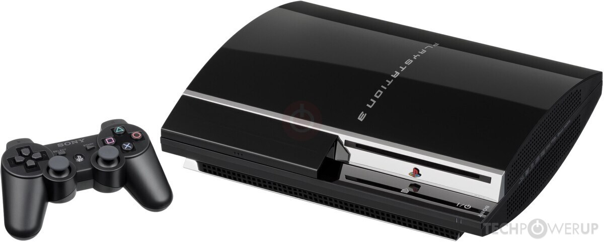
Front 2

Back
Recommended Gaming Resolutions:
- 640x480
- 1280x720
- 1366x768
The Playstation 3 GPU 65nm was a high-end gaming console graphics solution by NVIDIA, launched in August 2008. Built on the 65 nm process, and based on the RSX-65nm graphics processor, in its RSX-CXD2991 variant, the device does not support DirectX. The RSX-65nm graphics processor is an average sized chip with a die area of 186 mm² and 300 million transistors. It features 24 pixel shaders and 8 vertex shaders, 24 texture mapping units, and 8 ROPs. NVIDIA includes 256 MB GDDR3 memory, which are connected using a 128-bit memory interface. The GPU is operating at a frequency of 550 MHz, memory is running at 650 MHz.
Its power draw is rated at 58 W maximum. The console's dimensions are 325 mm x 98 mm x 274 mm, and it features a igp cooling solution. Its price at launch was 499 US Dollars.
Its power draw is rated at 58 W maximum. The console's dimensions are 325 mm x 98 mm x 274 mm, and it features a igp cooling solution. Its price at launch was 499 US Dollars.
Graphics Processor
Graphics Card
Clock Speeds
- GPU Clock
- 550 MHz
- Memory Clock
-
650 MHz
1300 Mbps effective
Memory
- Memory Size
- 256 MB
- Memory Type
- GDDR3
- Memory Bus
- 128 bit
- Bandwidth
- 20.80 GB/s
Render Config
- Pixel Shaders
- 24
- Vertex Shaders
- 8
- TMUs
- 24
- ROPs
- 8
Theoretical Performance
- Pixel Rate
- 4.400 GPixel/s
- Vertex Rate
- 1.100 GVertices/s
- Texture Rate
- 13.20 GTexel/s
Board Design
- Length
- 325 mm
12.8 inches
- Width
- 98 mm
3.9 inches
- Height
- 274 mm
10.8 inches
- Weight
- 5.0 kg (11.0 lbs)
- TDP
- 58 W
- Outputs
- 1x HDMI 1.3
Graphics Features
- DirectX
- N/A
- OpenGL
- ES 1.1
- OpenCL
- N/A
- Vulkan
- N/A
- Pixel Shader
- 3.0
- Vertex Shader
- 3.0
Console Notes
| Playstation 3 (3rd Generation) 40GB CECHJxx = November, 2007 80GB CECHKxx = August, 2008 80GB CECHLxx = August, 2008 80GB CECHMxx = October, 2008 160GB CECHPxx = October, 2008 160GB CECHQxx = November, 2008 Playstation 3 Slim (4th Generation) 120GB CECH-20xxA = September 1st, 2009 250GB CECH-20xxB = September 1st, 2009 |
RSX-65nm GPU Notes
| Multi-way programmable parallel floating-point shader pipelines Independent pixel/vertex shader architecture 24 parallel pixel-shader ALU pipes clocked @ 550 MHz 5 ALU operations per pipeline, per cycle - 2 vector4 - 2 scalar/dual/co-issue and fog ALU - 1 Texture ALU 16 floating-point operations per pipeline, per cycle Pixel Floating Point Operations: 211.2 GFLOPS (550MHz x 24 Shaders x 16 ops per clock per cycle) 8 parallel vertex pipelines @ 500 MHz 2 ALU operations per pipeline, per cycle - 1 vector4 - 1 scalar, dual issue 10 floating-point operations per pipeline, per cycle Vertex Floating Point Operations: 40.0 GFLOPS (500MHz x 8 Shaders x 10 ops per clock per cycle) Total Floating Point Operations: 251.2 GFLOPS (550MHz x 24 Shaders x 16 ops per clock per cycle) +(500MHz x 8 Shaders x 10 ops per clock per cycle) 74.0 billion shader operations/s (24 Pixel Shader Pipelines x 5 ALUs x 550 MHz) +(8 Vertex Shader Pipelines x 2 ALUs x 500 MHz) 24 texture filtering units (TF) 8 vertex texture addressing units (TA) 24 filtered samples per clock Peak texel fillrate: 13.2 GTexel/s (24 textures x 550 MHz) 32 unfiltered texture samples per clock (8 TA x 4 texture samples) 8 Render Output units / pixel rendering pipelines Peak pixel fillrate: 4.4 GPixel/s (8 ROPs x 550 MHz) Peak Z sample rate: 8.8 GSamples/s (2 Z-samples x 8 ROPs x 550 MHz) Peak Dot product operations: 56 billion/s (combined with Cell CPU) 128-bit pixel precision offers rendering of scenes with High dynamic range rendering (HDR) Cell FlexIO bus interface 20 GB/s read to the Cell and XDR memory 15 GB/s write to the Cell and XDR memory Support for PSGL (OpenGL ES 1.1 + Nvidia Cg) Support for S3TC texture compression |
May 21st, 2025 19:24 EDT
change timezone
Latest GPU Drivers
New Forum Posts
- as an AMD fanboy, I gotta say Nvidia's multi frame gen is just lit, even at 1080p (123)
- PSU recommendation for RTX 5090 (113)
- X79 and/or rampage IV OC'ing thread for those of us still left.... (2400)
- Ad blockers (27)
- Constant "EDP Other" under RING in ThrottleStop (265)
- Expedition 33 (19)
- Oblivion Remastered (79)
- Show your family how to check if a QR code is safe (8)
- Tower Server Case Recommendations (5)
- Post Your CyberPunk 2077 Benchmark (2024 edition) (137)
Popular Reviews
- ASRock B850 Steel Legend Wi-Fi Review
- DOOM: The Dark Ages Performance Benchmark Review - 40 GPUs Tested
- Upcoming Hardware Launches 2025 (Updated May 2025)
- Phison PASCARI X200E 6.4 TB Review
- PNY GeForce RTX 5070 Ti Epic-X RGB Plus OC Review
- Clair Obscur: Expedition 33 Performance Benchmark Review - 33 GPUs Tested
- Sapphire Radeon RX 9070 XT Nitro+ Review - Beating NVIDIA
- Fractal Design Meshify 3 Ambience Pro RGB Review
- AMD Ryzen 7 9800X3D Review - The Best Gaming Processor
- Raijintek AMPERE 1200 W Review
Controversial News Posts
- AMD Radeon RX 9060 XT to Roll Out 8 GB GDDR6 Edition, Despite Rumors (145)
- Microsoft Forces Automatic Windows 11 24H2 Update on Pro and Home PCs (121)
- XFX & Acer Radeon RX 9060 XT Graphics Cards Leaked by Retailers - Starting at "$450" (118)
- AMD "Zen 7" Rumors: Three Core Classes, 2 MB L2, 7 MB V‑Cache, and TSMC A14 Node (91)
- Parts of NVIDIA GeForce RTX 50 Series GPU PCB Reach Over 100°C: Report (85)
- NVIDIA Reportedly Working on GeForce RTX 5080 SUPER 24 GB & RTX 5070 SUPER 18 GB Designs (76)
- Intel Partner Prepares Dual Arc "Battlemage" B580 GPU with 48 GB of VRAM (64)
- NVIDIA Reportedly Limiting Press Access to GeForce RTX 5060 Drivers - Suggesting Late Arrival of Reviews (62)