Report an Error


NVIDIA GeForce GT 710
- Graphics Processor
- GK208B
- Cores
- 192
- TMUs
- 16
- ROPs
- 8
- Memory Size
- 2 GB
- Memory Type
- DDR3
- Bus Width
- 64 bit

GPU
Recommended Gaming Resolutions:
- 640x480
- 1280x720
- 1366x768
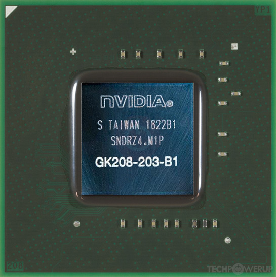
The GeForce GT 710 was a graphics card by NVIDIA, launched on March 27th, 2014. Built on the 28 nm process, and based on the GK208B graphics processor, in its GK208-203-B1 variant, the card supports DirectX 12. Even though it supports DirectX 12, the feature level is only 11_0, which can be problematic with newer DirectX 12 titles. The GK208B graphics processor is a relatively small chip with a die area of only 87 mm² and 1,020 million transistors. Unlike the fully unlocked GeForce GT 730, which uses the same GPU but has all 384 shaders enabled, NVIDIA has disabled some shading units on the GeForce GT 710 to reach the product's target shader count. It features 192 shading units, 16 texture mapping units, and 8 ROPs. NVIDIA has paired 2,048 MB DDR3 memory with the GeForce GT 710, which are connected using a 64-bit memory interface. The GPU is operating at a frequency of 954 MHz, memory is running at 900 MHz.
Being a single-slot card, the NVIDIA GeForce GT 710 does not require any additional power connector, its power draw is rated at 19 W maximum. Display outputs include: 1x DVI, 1x HDMI 1.4a, 1x VGA. GeForce GT 710 is connected to the rest of the system using a PCI-Express 2.0 x8 interface. The card measures 145 mm in length, and features a single-slot cooling solution.
Being a single-slot card, the NVIDIA GeForce GT 710 does not require any additional power connector, its power draw is rated at 19 W maximum. Display outputs include: 1x DVI, 1x HDMI 1.4a, 1x VGA. GeForce GT 710 is connected to the rest of the system using a PCI-Express 2.0 x8 interface. The card measures 145 mm in length, and features a single-slot cooling solution.
Graphics Processor
- GPU Name
- GK208B
- GPU Variant
- GK208-203-B1
- Architecture
- Kepler 2.0
- Foundry
- TSMC
- Process Size
- 28 nm
- Transistors
- 1,020 million
- Density
- 11.7M / mm²
- Die Size
- 87 mm²
- Chip Package
- FCBGA-595
Graphics Card
- Release Date
- Mar 27th, 2014
- Generation
- GeForce 700
- Predecessor
- GeForce 600
- Successor
- GeForce 900
- Production
- End-of-life
- Bus Interface
- PCIe 2.0 x8
Clock Speeds
- GPU Clock
- 954 MHz
- Memory Clock
-
900 MHz
1800 Mbps effective
Memory
- Memory Size
- 2 GB
- Memory Type
- DDR3
- Memory Bus
- 64 bit
- Bandwidth
- 14.40 GB/s
Render Config
- Shading Units
- 192
- TMUs
- 16
- ROPs
- 8
- SMX Count
- 1
- L1 Cache
- 16 KB (per SMX)
- L2 Cache
- 512 KB
Theoretical Performance
- Pixel Rate
- 3.816 GPixel/s
- Texture Rate
- 15.26 GTexel/s
- FP32 (float)
- 366.3 GFLOPS
- FP64 (double)
- 15.26 GFLOPS (1:24)
Board Design
- Slot Width
- Single-slot
- Length
- 145 mm
5.7 inches
- TDP
- 19 W
- Suggested PSU
- 200 W
- Outputs
- 1x DVI
1x HDMI 1.4a
1x VGA
- Power Connectors
- None
- Board Number
- P2132 SKU 12,
P2132 SKU 14
Graphics Features
- DirectX
- 12 (11_0)
- OpenGL
- 4.6
- OpenCL
- 3.0
- Vulkan
- 1.2.175
- CUDA
- 3.5
- Shader Model
- 6.5 (5.1)
GK208B GPU Notes
| NVENC: NVDEC: 1st Gen PureVideo HD: VP5 VDPAU: Feature Set D L1 Cache is configurable from 16 KB up to 48 KB per SMX Latest Drivers: Windows XP / Server 2003 x64: GeForce Release 368.81 Quadro Release R319 U2 (321.01) Windows Vista: GeForce Release 365.19 Quadro Release R346 U7 (348.40) / R352 BETA (352.86) Windows 7 / 8 / 8.1 / 10 / 11 (x32 / x64): GeForce Release 391.35 / 474.89 Quadro Release R390 U9 (392.37) / R470 U16 (474.82) Quadro Mobile Release R390 U9 (392.37) / R418 U9 (426.78) |
Retail boards based on this design (11)
| Name | GPU Clock | Memory Clock | Other Changes |
|---|---|---|---|
| 954 MHz | 1253 MHz | GDDR5, 167 mm/6.6 inches, 4x HDMI | |
| 954 MHz | 900 MHz | 1024 MB, 114 mm/4.5 inches, 2x DVI 1x mini-HDMI | |
| 954 MHz | 900 MHz | 114 mm/4.5 inches, 2x DVI 1x mini-HDMI | |
| 954 MHz | 900 MHz | 1024 MB, 114 mm/4.5 inches | |
| 954 MHz | 900 MHz | 114 mm/4.5 inches | |
| 954 MHz | 900 MHz | 1024 MB, 114 mm/4.5 inches | |
| 954 MHz | 900 MHz | 114 mm/4.5 inches | |
| 954 MHz | 900 MHz | 1024 MB, 144 mm/5.7 inches | |
| 954 MHz | 800 MHz | 1024 MB, 140 mm/5.5 inches | |
| 954 MHz | 800 MHz | 1024 MB, 146 mm/5.7 inches | |
| 954 MHz | 800 MHz |


Apr 25th, 2025 03:33 EDT
change timezone
Latest GPU Drivers
New Forum Posts
- Help getting a mini pc (11)
- To distill or not distill what say ye? (101)
- AMD RX 9070 XT & RX 9070 non-XT thread (OC, undervolt, benchmarks, ...) (100)
- RX 9000 series GPU Owners Club (525)
- Asus Rx570 o4g cannot losd drivers error code 43 (19)
- Help Flash MI50 to Radeon VII Pro (22)
- New OLED monitor makes PC unresponsive sometimes (31)
- pc randomly blackscreening (1)
- V/F Points not being respected consistantly (10)
- Are the 8 GB cards worth it? (179)
Popular Reviews
- NVIDIA GeForce RTX 5060 Ti 8 GB Review - So Many Compromises
- Crucial CUDIMM DDR5-6400 128 GB CL52 Review
- Colorful iGame B860M Ultra V20 Review
- ASUS GeForce RTX 5060 Ti TUF OC 16 GB Review
- Upcoming Hardware Launches 2025 (Updated Apr 2025)
- Sapphire Radeon RX 9070 XT Pulse Review
- Sapphire Radeon RX 9070 XT Nitro+ Review - Beating NVIDIA
- ASRock X870E Taichi Lite Review
- AMD Ryzen 7 9800X3D Review - The Best Gaming Processor
- ASUS GeForce RTX 5080 TUF OC Review
Controversial News Posts
- NVIDIA GeForce RTX 5060 Ti 16 GB SKU Likely Launching at $499, According to Supply Chain Leak (182)
- NVIDIA Sends MSRP Numbers to Partners: GeForce RTX 5060 Ti 8 GB at $379, RTX 5060 Ti 16 GB at $429 (127)
- NVIDIA Launches GeForce RTX 5060 Series, Beginning with RTX 5060 Ti This Week (115)
- Nintendo Confirms That Switch 2 Joy-Cons Will Not Utilize Hall Effect Stick Technology (105)
- Nintendo Switch 2 Launches June 5 at $449.99 with New Hardware and Games (99)
- Sony Increases the PS5 Pricing in EMEA and ANZ by Around 25 Percent (84)
- NVIDIA PhysX and Flow Made Fully Open-Source (77)
- Windows Notepad Gets Microsoft Copilot Integration (75)