Report an Error


NVIDIA GeForce GT 720
- Graphics Processor
- GK208B
- Cores
- 192
- TMUs
- 16
- ROPs
- 8
- Memory Size
- 1024 MB
- Memory Type
- DDR3
- Bus Width
- 64 bit

GPU
Recommended Gaming Resolutions:
- 640x480
- 1280x720
- 1366x768
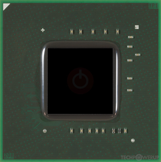
The GeForce GT 720 was an entry-level graphics card by NVIDIA, launched on September 29th, 2014. Built on the 28 nm process, and based on the GK208B graphics processor, the card supports DirectX 12. Even though it supports DirectX 12, the feature level is only 11_0, which can be problematic with newer DirectX 12 titles. The GK208B graphics processor is a relatively small chip with a die area of only 87 mm² and 1,020 million transistors. Unlike the fully unlocked GeForce GT 730, which uses the same GPU but has all 384 shaders enabled, NVIDIA has disabled some shading units on the GeForce GT 720 to reach the product's target shader count. It features 192 shading units, 16 texture mapping units, and 8 ROPs. NVIDIA has paired 1,024 MB DDR3 memory with the GeForce GT 720, which are connected using a 64-bit memory interface. The GPU is operating at a frequency of 797 MHz, memory is running at 800 MHz.
Being a single-slot card, the NVIDIA GeForce GT 720 does not require any additional power connector, its power draw is rated at 19 W maximum. Display outputs include: 1x DVI, 1x HDMI 1.4a, 1x VGA. GeForce GT 720 is connected to the rest of the system using a PCI-Express 2.0 x8 interface. The card measures 145 mm in length, and features a single-slot cooling solution. Its price at launch was 49 US Dollars.
Being a single-slot card, the NVIDIA GeForce GT 720 does not require any additional power connector, its power draw is rated at 19 W maximum. Display outputs include: 1x DVI, 1x HDMI 1.4a, 1x VGA. GeForce GT 720 is connected to the rest of the system using a PCI-Express 2.0 x8 interface. The card measures 145 mm in length, and features a single-slot cooling solution. Its price at launch was 49 US Dollars.
Graphics Processor
- GPU Name
- GK208B
- Architecture
- Kepler 2.0
- Foundry
- TSMC
- Process Size
- 28 nm
- Transistors
- 1,020 million
- Density
- 11.7M / mm²
- Die Size
- 87 mm²
- Chip Package
- FCBGA-595
Graphics Card
- Release Date
- Sep 29th, 2014
- Generation
- GeForce 700
- Predecessor
- GeForce 600
- Successor
- GeForce 900
- Production
- End-of-life
- Launch Price
- 49 USD
- Bus Interface
- PCIe 2.0 x8
Clock Speeds
- GPU Clock
- 797 MHz
- Memory Clock
-
800 MHz
1600 Mbps effective
Memory
- Memory Size
- 1024 MB
- Memory Type
- DDR3
- Memory Bus
- 64 bit
- Bandwidth
- 12.80 GB/s
Render Config
- Shading Units
- 192
- TMUs
- 16
- ROPs
- 8
- SMX Count
- 1
- L1 Cache
- 16 KB (per SMX)
- L2 Cache
- 512 KB
Theoretical Performance
- Pixel Rate
- 3.188 GPixel/s
- Texture Rate
- 12.75 GTexel/s
- FP32 (float)
- 306.0 GFLOPS
- FP64 (double)
- 12.75 GFLOPS (1:24)
Board Design
- Slot Width
- Single-slot
- Length
- 145 mm
5.7 inches
- TDP
- 19 W
- Suggested PSU
- 200 W
- Outputs
- 1x DVI
1x HDMI 1.4a
1x VGA
- Power Connectors
- None
- Board Number
- P2131 SKU 10,
P2132 SKU 11
Graphics Features
- DirectX
- 12 (11_0)
- OpenGL
- 4.6
- OpenCL
- 3.0
- Vulkan
- 1.2.175
- CUDA
- 3.5
- Shader Model
- 6.5 (5.1)
GK208B GPU Notes
| NVENC: NVDEC: 1st Gen PureVideo HD: VP5 VDPAU: Feature Set D L1 Cache is configurable from 16 KB up to 48 KB per SMX Latest Drivers: Windows XP / Server 2003 x64: GeForce Release 368.81 Quadro Release R319 U2 (321.01) Windows Vista: GeForce Release 365.19 Quadro Release R346 U7 (348.40) / R352 BETA (352.86) Windows 7 / 8 / 8.1 / 10 / 11 (x32 / x64): GeForce Release 391.35 / 474.89 Quadro Release R390 U9 (392.37) / R470 U16 (474.82) Quadro Mobile Release R390 U9 (392.37) / R418 U9 (426.78) |
Retail boards based on this design (2)
| Name | GPU Clock | Memory Clock | Other Changes |
|---|---|---|---|
| 797 MHz | 800 MHz | 2 GB, 162 mm/6.4 inches | |
| 797 MHz | 900 MHz | 1x DVI 1x VGA |


Jun 28th, 2025 17:29 CDT
change timezone
Latest GPU Drivers
New Forum Posts
- Best time to sell your used 4090s is now. (256)
- Bitlocker doesnt auto-unlock ext drive (2)
- SLI is really not Dead if you Have a SLI rig (116)
- What air cooler should I get for Jonsbo Z20-9800X3D? (5)
- X79 and/or rampage IV OC'ing thread for those of us still left.... (2418)
- Page loading issues from Russia (50)
- Can anyone recomend a video course on basic computer repair? (39)
- Kingston WI-Drive 128GB looking ill today!! (14)
- The TPU UK Clubhouse (26503)
- Can you guess Which game it is? (187)
Popular Reviews
- ASRock Phantom Gaming Z890 Riptide Wi-Fi Review
- Sapphire Radeon RX 9060 XT Pulse OC 16 GB Review - Samsung Memory Tested
- SCHENKER KEY 18 Pro (E25) Review - Top-Tier Contender
- Lexar NQ780 4 TB Review
- AMD Ryzen 7 9800X3D Review - The Best Gaming Processor
- Upcoming Hardware Launches 2025 (Updated May 2025)
- AVerMedia CamStream 4K Review
- Sapphire Radeon RX 9070 XT Nitro+ Review - Beating NVIDIA
- NVIDIA GeForce RTX 5060 8 GB Review
- Intel Core Ultra 7 265K Review
TPU on YouTube
Controversial News Posts
- Intel's Core Ultra 7 265K and 265KF CPUs Dip Below $250 (287)
- NVIDIA Grabs Market Share, AMD Loses Ground, and Intel Disappears in Latest dGPU Update (204)
- Microsoft Partners with AMD for Next-gen Xbox Hardware (105)
- NVIDIA Launches GeForce RTX 5050 for Desktops and Laptops, Starts at $249 (101)
- Intel "Nova Lake‑S" Series: Seven SKUs, Up to 52 Cores and 150 W TDP (100)
- Reviewers Bemused by Restrictive Sampling of RX 9060 XT 8 GB Cards (88)
- NVIDIA GeForce RTX 5050 Reportedly Scheduled for July Release (87)
- GPU IPC Showdown: NVIDIA Blackwell vs Ada Lovelace; AMD RDNA 4 vs RDNA 3 (79)