Report an Error


NVIDIA GeForce PCX 5750
- Graphics Processor
- NV39
- Pixel Shaders
- 4
- Vertex Shaders
- 3
- TMUs
- 4
- ROPs
- 4
- Memory Size
- 128 MB
- Memory Type
- DDR
- Bus Width
- 128 bit

GPU
Recommended Gaming Resolutions:
- 640x480
- 1280x720
- 1366x768
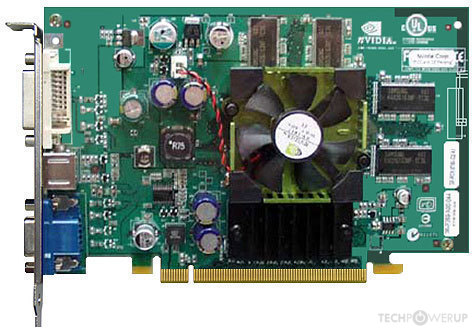
The GeForce PCX 5750 was a graphics card by NVIDIA, launched on February 17th, 2004. Built on the 130 nm process, and based on the NV39 graphics processor, in its FX 5700 variant, the card supports DirectX 9.0a. Since GeForce PCX 5750 does not support DirectX 11 or DirectX 12, it might not be able to run all the latest games. The NV39 graphics processor is an average sized chip with a die area of 125 mm² and 82 million transistors. It features 4 pixel shaders and 3 vertex shaders, 4 texture mapping units, and 4 ROPs. Due to the lack of unified shaders you will not be able to run recent games at all (which require unified shader/DX10+ support). NVIDIA has paired 128 MB DDR memory with the GeForce PCX 5750, which are connected using a 128-bit memory interface. The GPU is operating at a frequency of 425 MHz, memory is running at 275 MHz.
Being a single-slot card, the NVIDIA GeForce PCX 5750 does not require any additional power connector, its power draw is rated at 50 W maximum. Display outputs include: 1x DVI, 1x VGA, 1x S-Video. GeForce PCX 5750 is connected to the rest of the system using a PCI-Express 1.0 x16 interface. The card measures 168 mm in length, and features a single-slot cooling solution.
Being a single-slot card, the NVIDIA GeForce PCX 5750 does not require any additional power connector, its power draw is rated at 50 W maximum. Display outputs include: 1x DVI, 1x VGA, 1x S-Video. GeForce PCX 5750 is connected to the rest of the system using a PCI-Express 1.0 x16 interface. The card measures 168 mm in length, and features a single-slot cooling solution.
Graphics Processor
Graphics Card
- Release Date
- Feb 17th, 2004
- Generation
- GeForce PCX
- Predecessor
- GeForce 4 Ti
- Successor
- GeForce 6 PCIe
- Production
- End-of-life
- Bus Interface
- PCIe 1.0 x16
- Reviews
- 8 in our database
Clock Speeds
- GPU Clock
- 425 MHz
- Memory Clock
-
275 MHz
550 Mbps effective
Memory
- Memory Size
- 128 MB
- Memory Type
- DDR
- Memory Bus
- 128 bit
- Bandwidth
- 8.800 GB/s
Render Config
- Pixel Shaders
- 4
- Vertex Shaders
- 3
- TMUs
- 4
- ROPs
- 4
Theoretical Performance
- Pixel Rate
- 1.700 GPixel/s
- Vertex Rate
- 318.8 MVertices/s
- Texture Rate
- 1.700 GTexel/s
Board Design
- Slot Width
- Single-slot
- Length
- 168 mm
6.6 inches
- TDP
- 50 W
- Suggested PSU
- 250 W
- Outputs
- 1x DVI
1x VGA
1x S-Video
- Power Connectors
- None
Graphics Features
- DirectX
- 9.0a
- OpenGL
-
1.5 (full)
2.0 (partial)
- OpenCL
- N/A
- Vulkan
- N/A
- Pixel Shader
- 2.0a
- Vertex Shader
- 2.0a
NV39 GPU Notes
| NV39 = NV36 + PCI-Bridge |
Retail boards based on this design (1)
| Name | GPU Clock | Memory Clock | Other Changes |
|---|---|---|---|
| 425 MHz | 275 MHz |

Apr 26th, 2024 13:32 EDT
change timezone
Latest GPU Drivers
New Forum Posts
- DTS:X APO4 + DTS Interactive for Most Devices [USB Supported] (305)
- The Official Linux/Unix Desktop Screenshots Megathread (702)
- What's your latest tech purchase? (20352)
- hacked (73)
- im new to throttelstop and i think i messed it up by copying others any hints would be very much aprreciated (5)
- 2022-X58/1366 PIN Motherboards NVME M.2 SSD BIOS MOD Collection (657)
- DTS DCH Driver for Realtek HDA [DTS:X APO4 + DTS Interactive] (1909)
- checkup (1)
- Help me to OC my 5700X (10)
- XFX RX470 8GB no video and error 43 (28)
Popular Reviews
- HYTE THICC Q60 240 mm AIO Review
- MOONDROP x Crinacle DUSK In-Ear Monitors Review - The Last 5%
- Alienware Pro Wireless Gaming Keyboard Review
- Upcoming Hardware Launches 2023 (Updated Feb 2024)
- Thermalright Phantom Spirit 120 EVO Review
- FiiO K19 Desktop DAC/Headphone Amplifier Review
- ASUS Radeon RX 7900 GRE TUF OC Review
- RTX 4090 & 53 Games: Ryzen 7 5800X vs Ryzen 7 5800X3D Review
- NVIDIA RTX 4090: 450 W vs 600 W 12VHPWR - Is there any notable performance difference?
- AMD Ryzen 7 7800X3D Review - The Best Gaming CPU
Controversial News Posts
- Windows 11 Now Officially Adware as Microsoft Embeds Ads in the Start Menu (128)
- Sony PlayStation 5 Pro Specifications Confirmed, Console Arrives Before Holidays (117)
- NVIDIA Points Intel Raptor Lake CPU Users to Get Help from Intel Amid System Instability Issues (106)
- AMD "Strix Halo" Zen 5 Mobile Processor Pictured: Chiplet-based, Uses 256-bit LPDDR5X (102)
- US Government Wants Nuclear Plants to Offload AI Data Center Expansion (98)
- AMD's RDNA 4 GPUs Could Stick with 18 Gbps GDDR6 Memory (92)
- Developers of Outpost Infinity Siege Recommend Underclocking i9-13900K and i9-14900K for Stability on Machines with RTX 4090 (85)
- Windows 10 Security Updates to Cost $61 After 2025, $427 by 2028 (84)