Report an Error


ATI FireGL V5000
- Graphics Processor
- RV410
- Pixel Shaders
- 8
- Vertex Shaders
- 6
- TMUs
- 8
- ROPs
- 8
- Memory Size
- 128 MB
- Memory Type
- GDDR3
- Bus Width
- 128 bit
GPU

I/O
Recommended Gaming Resolutions:
- 640x480
- 1280x720
- 1366x768
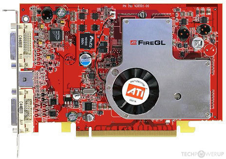
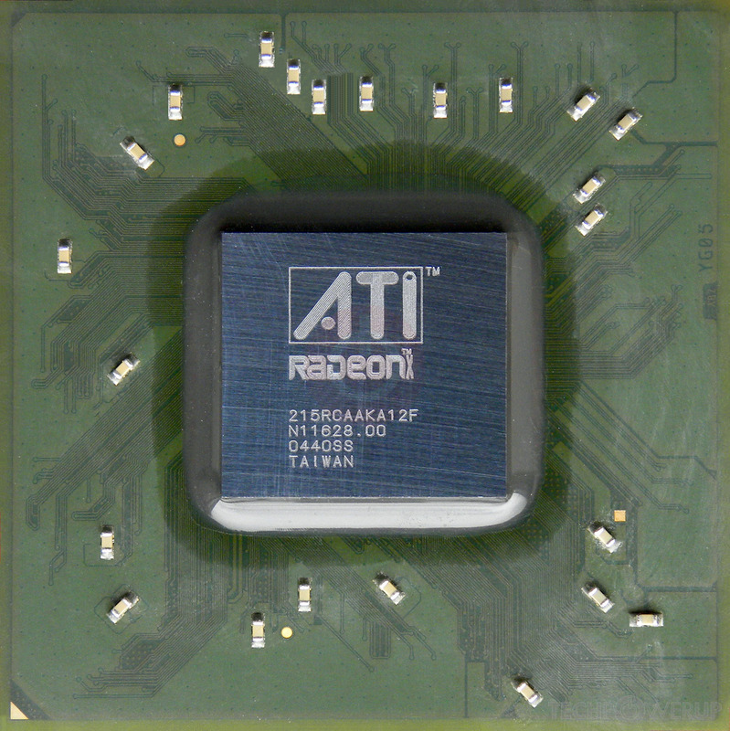
The FireGL V5000 was an enthusiast-class professional graphics card by ATI, launched on September 1st, 2004. Built on the 110 nm process, and based on the RV410 graphics processor, in its RV410 GL variant, the card supports DirectX 9.0b. Since FireGL V5000 does not support DirectX 11 or DirectX 12, it might not be able to run all the latest games. The RV410 graphics processor is an average sized chip with a die area of 156 mm² and 120 million transistors. It features 8 pixel shaders and 6 vertex shaders, 8 texture mapping units, and 8 ROPs. Due to the lack of unified shaders you will not be able to run recent games at all (which require unified shader/DX10+ support). ATI has paired 128 MB GDDR3 memory with the FireGL V5000, which are connected using a 128-bit memory interface. The GPU is operating at a frequency of 425 MHz, memory is running at 430 MHz.
Being a single-slot card, the ATI FireGL V5000 does not require any additional power connector, its power draw is not exactly known. Display outputs include: 2x DVI, 1x S-Video. FireGL V5000 is connected to the rest of the system using a PCI-Express 1.0 x16 interface. The card measures 183 mm in length, 111 mm in width, and features a single-slot cooling solution. Its price at launch was 699 US Dollars.
Being a single-slot card, the ATI FireGL V5000 does not require any additional power connector, its power draw is not exactly known. Display outputs include: 2x DVI, 1x S-Video. FireGL V5000 is connected to the rest of the system using a PCI-Express 1.0 x16 interface. The card measures 183 mm in length, 111 mm in width, and features a single-slot cooling solution. Its price at launch was 699 US Dollars.
Graphics Processor
Graphics Card
- Release Date
- Sep 1st, 2004
- Generation
-
FireGL
(Vx000)
- Predecessor
- Fire GL
- Successor
- FirePro Terascale
- Production
- End-of-life
- Launch Price
- 699 USD
- Bus Interface
- PCIe 1.0 x16
- Reviews
- 5 in our database
Clock Speeds
- GPU Clock
- 425 MHz
- Memory Clock
-
430 MHz
860 Mbps effective
Memory
- Memory Size
- 128 MB
- Memory Type
- GDDR3
- Memory Bus
- 128 bit
- Bandwidth
- 13.76 GB/s
Render Config
- Pixel Shaders
- 8
- Vertex Shaders
- 6
- TMUs
- 8
- ROPs
- 8
Theoretical Performance
- Pixel Rate
- 3.400 GPixel/s
- Vertex Rate
- 637.5 MVertices/s
- Texture Rate
- 3.400 GTexel/s
Board Design
- Slot Width
- Single-slot
- Length
- 183 mm
7.2 inches
- Width
- 111 mm
4.4 inches
- TDP
- unknown
- Suggested PSU
- 200 W
- Outputs
- 2x DVI
1x S-Video
- Power Connectors
- None
- Board Number
- 109-A38501-00
Graphics Features
- DirectX
- 9.0b (9_2)
- OpenGL
- 2.0
- OpenCL
- N/A
- Vulkan
- N/A
- Pixel Shader
- 2.0b
- Vertex Shader
- 2.0b
RV410 GPU Notes
| Mobile Variant: M26 Codename: Alto Graphics/Compute: GFX2 Smart Shader HD Smooth Vision HD TruForm 2.0 Hyper Z HD Video Shader HD 3Dc Compression Programmable pixel&vertex pipelines |
May 11th, 2024 02:43 EDT
change timezone
Latest GPU Drivers
New Forum Posts
- AM5 boot times improve RADICALLY with memory context restore enabled (40)
- NVME underperforming (4)
- 2024 and STILL no dark mode? (14)
- Windows 7 Club (1022)
- Moving from test bench to my PC case soon, but I am missing standoffs and the right screws for the standoffs (0)
- Dell Workstation Owners Club (3075)
- LOL ASUS says this is $200 in repair, Steve from gamers Nexus smokes ASUS, Steam Deck til I die boys!!!! (25)
- The Filthy, Rotten, Nasty, Helpdesk-Nightmare picture clubhouse (2624)
- Battery swap for cyberpower UPS (83)
- TPU's WCG/BOINC Team (34426)
Popular Reviews
- Bykski CPU-XPR-C-I CPU Water Block Review - Amazing Value!
- CHERRY XTRFY M64 Pro Review
- ThundeRobot ML903 NearLink Review
- ZMF Caldera Closed Planar Magnetic Headphones Review
- Corsair MP700 Pro SE 4 TB Review
- Corsair iCUE Link RX120 RGB 120 mm Fan Review
- Upcoming Hardware Launches 2023 (Updated Feb 2024)
- AMD Ryzen 7 7800X3D Review - The Best Gaming CPU
- Finalmouse UltralightX Review
- ASUS Radeon RX 7900 GRE TUF OC Review
Controversial News Posts
- Intel Statement on Stability Issues: "Motherboard Makers to Blame" (264)
- AMD to Redesign Ray Tracing Hardware on RDNA 4 (206)
- Windows 11 Now Officially Adware as Microsoft Embeds Ads in the Start Menu (171)
- NVIDIA to Only Launch the Flagship GeForce RTX 5090 in 2024, Rest of the Series in 2025 (144)
- Sony PlayStation 5 Pro Specifications Confirmed, Console Arrives Before Holidays (119)
- AMD's RDNA 4 GPUs Could Stick with 18 Gbps GDDR6 Memory (114)
- NVIDIA Points Intel Raptor Lake CPU Users to Get Help from Intel Amid System Instability Issues (106)
- AMD Ryzen 9 7900X3D Now at a Mouth-watering $329 (104)