Report an Error
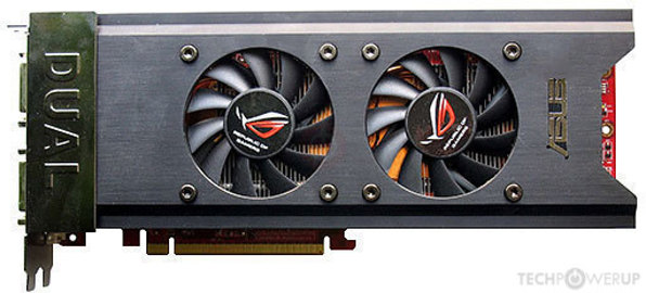

ASUS ROG HD 3870 X2 TOP
- EAH3870X2-TOP/G/3DHTI/1G
- Graphics Processor
- R680 x2
- Cores
- 320 x2
- TMUs
- 16 x2
- ROPs
- 16 x2
- Memory Size
- 512 MB x2
- Memory Type
- GDDR3
- Bus Width
- 256 bit x2


GPU
Graphics Processor
Graphics Card
- Release Date
- Jan 26th, 2008
- Generation
-
Radeon R600
(HD 3800)
- Predecessor
- Radeon R500 PCIe
- Successor
- Radeon R700
- Production
- End-of-life
- Bus Interface
- PCIe 2.0 x16
Clock Speeds
- GPU Clock
825 MHz
851 MHz (+3%)
- Memory Clock
-
901 MHz
954 MHz (+6%)
1802 Mbps effective
1908 Mbps effective
Memory
- Memory Size
- 512 MB
- Memory Type
- GDDR3
- Memory Bus
- 256 bit
- Bandwidth
-
57.66 GB/s
61.06 GB/s
Render Config
- Shading Units
- 320
- TMUs
- 16
- ROPs
- 16
- Compute Units
- 4
- L2 Cache
- 256 KB
Theoretical Performance
- Pixel Rate
-
13.20 GPixel/s
13.62 GPixel/s
- Texture Rate
-
13.20 GTexel/s
13.62 GTexel/s
- FP32 (float)
-
528.0 GFLOPS
544.6 GFLOPS
- FP64 (double)
-
105.6 GFLOPS
108.9 GFLOPS (1:5)
Board Design
- Slot Width
- Dual-slot
- TDP
- 165 W
- Suggested PSU
- 450 W
- Outputs
2x DVI
1x S-Video
4x DVI
1x S-Video
- Power Connectors
- 1x 6-pin + 1x 8-pin
- Board Number
- 109-B40031-10
Graphics Features
- DirectX
- 10.1 (10_1)
- OpenGL
-
3.3 (full)
4.0 (partial)
- OpenCL
- N/A
- Vulkan
- N/A
- Shader Model
- 4.1
R680 GPU Notes
| Graphics/Compute: GFX3 Display Core Engine: 2.0 Unified Video Decoder: 1.0 OpenGL 4.0: 23% Support OpenGL 4.1: 71% Support OpenGL 4.2: 16% Support |
Other retail boards based on this design (3)
| Name | GPU Clock | Memory Clock | Other Changes |
|---|---|---|---|
|
ASUS ROG HD 3870 X2 TOP

|
851 MHz | 954 MHz | 4x DVI 1x S-Video |
| 825 MHz | 1125 MHz | GDDR4, 3x DVI 1x HDMI 1x S-Video | |
| 860 MHz | 931 MHz | Single-slot |


Apr 26th, 2024 17:56 EDT
change timezone
Latest GPU Drivers
New Forum Posts
- looking to build a new system and im considering asrock brand but i have some doubts/concerns. (5)
- TPU's Nostalgic Hardware Club (18474)
- What's your latest tech purchase? (20354)
- 5800x (and other Zen 3 chips) PBO settings/Temperature fix (934)
- Only EDP Other in Core? (2)
- Alphacool CORE 1 CPU block - bulging with danger of splitting? (30)
- Dell Workstation Owners Club (3061)
- Xeon Owners Club (8700)
- Secure boot already open help (10)
- hacked (77)
Popular Reviews
- HYTE THICC Q60 240 mm AIO Review
- MOONDROP x Crinacle DUSK In-Ear Monitors Review - The Last 5%
- Upcoming Hardware Launches 2023 (Updated Feb 2024)
- Alienware Pro Wireless Gaming Keyboard Review
- Thermalright Phantom Spirit 120 EVO Review
- FiiO K19 Desktop DAC/Headphone Amplifier Review
- ASUS Radeon RX 7900 GRE TUF OC Review
- Ugreen NASync DXP4800 Plus Review
- AMD Ryzen 7 7800X3D Review - The Best Gaming CPU
- Sapphire Radeon RX 7900 GRE Pulse Review
Controversial News Posts
- Windows 11 Now Officially Adware as Microsoft Embeds Ads in the Start Menu (135)
- Sony PlayStation 5 Pro Specifications Confirmed, Console Arrives Before Holidays (117)
- NVIDIA Points Intel Raptor Lake CPU Users to Get Help from Intel Amid System Instability Issues (106)
- AMD "Strix Halo" Zen 5 Mobile Processor Pictured: Chiplet-based, Uses 256-bit LPDDR5X (103)
- US Government Wants Nuclear Plants to Offload AI Data Center Expansion (98)
- AMD's RDNA 4 GPUs Could Stick with 18 Gbps GDDR6 Memory (95)
- Developers of Outpost Infinity Siege Recommend Underclocking i9-13900K and i9-14900K for Stability on Machines with RTX 4090 (85)
- Windows 10 Security Updates to Cost $61 After 2025, $427 by 2028 (84)