Report an Error


NVIDIA GeForce GT 640 OEM 1 GB
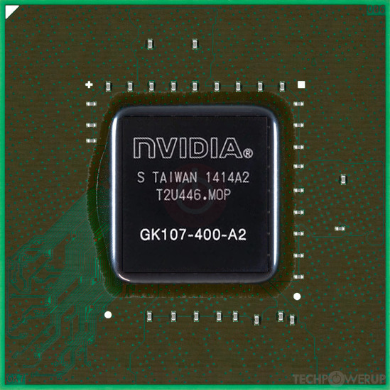
- Graphics Processor
- GK107
- Cores
- 384
- TMUs
- 32
- ROPs
- 16
- Memory Size
- 1024 MB
- Memory Type
- GDDR5
- Bus Width
- 128 bit
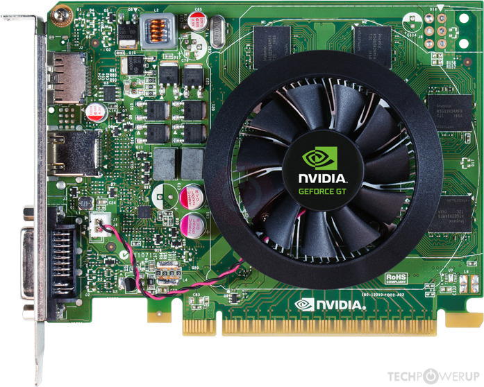
GPU

I/O

Bottom
Graphics Processor
Graphics Card
- Release Date
- Apr 24th, 2012
- Generation
- GeForce 600
- Predecessor
- GeForce 500
- Successor
- GeForce 700
- Production
- End-of-life
- Bus Interface
- PCIe 3.0 x16
Clock Speeds
- GPU Clock
797 MHz
954 MHz (+20%)
- Memory Clock
-
891 MHz
1250 MHz (+40%)
1782 Mbps effective
5 Gbps effective
Memory
- Memory Size
-
2 GB
1024 MB
- Memory Type
DDR3
GDDR5
- Memory Bus
- 128 bit
- Bandwidth
-
28.51 GB/s
80.00 GB/s
Render Config
- Shading Units
- 384
- TMUs
- 32
- ROPs
- 16
- SMX Count
- 2
- L1 Cache
- 16 KB (per SMX)
- L2 Cache
- 256 KB
Theoretical Performance
- Pixel Rate
-
6.376 GPixel/s
7.632 GPixel/s
- Texture Rate
-
25.50 GTexel/s
30.53 GTexel/s
- FP32 (float)
-
612.1 GFLOPS
732.7 GFLOPS
- FP64 (double)
-
25.50 GFLOPS
30.53 GFLOPS (1:24)
Board Design
- Slot Width
- Single-slot
- TDP
- 50 W
- Suggested PSU
- 250 W
- Outputs
- 1x DVI
1x HDMI 1.4a
1x DisplayPort 1.2
- Power Connectors
- None
- Board Number
- P2010 SKU 3,
P2010 SKU 6,
P2012 SKU 1,
P2012 SKU 3
Graphics Features
- DirectX
- 12 (11_0)
- OpenGL
- 4.6
- OpenCL
- 3.0
- Vulkan
- 1.2.175
- CUDA
- 3.0
- Shader Model
- 6.5 (5.1)
Card Notes
| Variant Memory: 4096MB DDR3 Variant Memory: 1024MB GDDR5 |
GK107 GPU Notes
| NVENC: 1st Gen NVDEC: 1st Gen PureVideo HD: VP5 VDPAU: Feature Set D L1 Cache is configurable from 16 KB up to 48 KB per SMX |
Other retail boards based on this design (4)
| Name | GPU Clock | Memory Clock | Other Changes |
|---|---|---|---|
| 797 MHz | 891 MHz | 4 GB | |
| 797 MHz | 891 MHz | 4 GB | |
|
NVIDIA GeForce GT 640 OEM 1 GB

|
954 MHz | 1250 MHz | 1024 MB, GDDR5 |
| 797 MHz | 891 MHz |


Apr 25th, 2024 23:17 EDT
change timezone
Latest GPU Drivers
New Forum Posts
- Black screen after muting (5)
- What phone you use as your daily driver? And, a discussion of them. (1481)
- What are you playing? (20530)
- Secure boot already open help (0)
- TPU's Nostalgic Hardware Club (18465)
- Post your Speedometer 3.0 Score (36)
- Size on Disk Excessively Different than Size (9)
- Dell Workstation Owners Club (3056)
- Core PL1 + GPU PL1 + Ring EDP OTHER (10)
- Best SSD for system drive (80)
Popular Reviews
- Fractal Design Terra Review
- Thermalright Phantom Spirit 120 EVO Review
- Corsair 2000D Airflow Review
- ASUS GeForce RTX 4090 STRIX OC Review
- NVIDIA GeForce RTX 4090 Founders Edition Review - Impressive Performance
- ASUS GeForce RTX 4090 Matrix Platinum Review - The RTX 4090 Ti
- MSI GeForce RTX 4090 Suprim X Review
- Gigabyte GeForce RTX 4090 Gaming OC Review
- MSI GeForce RTX 4090 Gaming X Trio Review
- MSI GeForce RTX 4090 Suprim Liquid X Review
Controversial News Posts
- Sony PlayStation 5 Pro Specifications Confirmed, Console Arrives Before Holidays (117)
- Windows 11 Now Officially Adware as Microsoft Embeds Ads in the Start Menu (110)
- NVIDIA Points Intel Raptor Lake CPU Users to Get Help from Intel Amid System Instability Issues (106)
- AMD "Strix Halo" Zen 5 Mobile Processor Pictured: Chiplet-based, Uses 256-bit LPDDR5X (101)
- US Government Wants Nuclear Plants to Offload AI Data Center Expansion (98)
- AMD's RDNA 4 GPUs Could Stick with 18 Gbps GDDR6 Memory (88)
- Developers of Outpost Infinity Siege Recommend Underclocking i9-13900K and i9-14900K for Stability on Machines with RTX 4090 (85)
- Windows 10 Security Updates to Cost $61 After 2025, $427 by 2028 (84)