Report an Error


Sapphire X700 Fireblade
- 100122
- Graphics Processor
- RV410
- Pixel Shaders
- 8
- Vertex Shaders
- 6
- TMUs
- 8
- ROPs
- 8
- Memory Size
- 256 MB
- Memory Type
- DDR
- Bus Width
- 128 bit

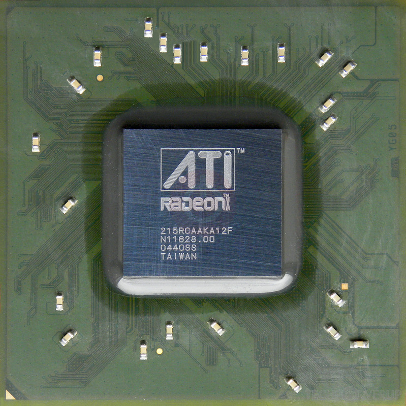
GPU
Graphics Processor
Graphics Card
- Release Date
Sep 1st, 2004
Jul 15th, 2005
- Generation
-
Radeon R400 PCIe
(X700)
- Predecessor
- Radeon R300
- Successor
- Radeon R500 PCIe
- Production
- End-of-life
- Bus Interface
- PCIe 1.0 x16
Clock Speeds
- GPU Clock
- 400 MHz
- Memory Clock
-
250 MHz
500 Mbps effective
Memory
- Memory Size
-
128 MB
256 MB
- Memory Type
- DDR
- Memory Bus
- 128 bit
- Bandwidth
- 8.000 GB/s
Render Config
- Pixel Shaders
- 8
- Vertex Shaders
- 6
- TMUs
- 8
- ROPs
- 8
Theoretical Performance
- Pixel Rate
- 3.200 GPixel/s
- Vertex Rate
- 600.0 MVertices/s
- Texture Rate
- 3.200 GTexel/s
Board Design
- Slot Width
- Single-slot
- TDP
- 44 W
- Suggested PSU
- 200 W
- Outputs
- 1x DVI
1x VGA
1x S-Video
- Power Connectors
- None
Graphics Features
- DirectX
- 9.0b (9_2)
- OpenGL
- 2.0
- OpenCL
- N/A
- Vulkan
- N/A
- Pixel Shader
- 2.0b
- Vertex Shader
- 2.0b
Card Notes
| Variant Memory: 256 MB |
RV410 GPU Notes
| Mobile Variant: M26 Codename: Alto Graphics/Compute: GFX2 Smart Shader HD Smooth Vision HD TruForm 2.0 Hyper Z HD Video Shader HD 3Dc Compression Programmable pixel&vertex pipelines |
Other retail boards based on this design (1)
| Name | GPU Clock | Memory Clock | Other Changes |
|---|---|---|---|
|
Sapphire X700 Fireblade

|
400 MHz | 250 MHz | 256 MB |
Apr 26th, 2024 00:54 EDT
change timezone
Latest GPU Drivers
New Forum Posts
- What's your latest tech purchase? (20341)
- Horizontal black lines popping up on my screen? (0)
- Which new games will you be buying? (316)
- Alphacool CORE 1 CPU block - bulging with danger of splitting? (20)
- Black screen after muting (5)
- What phone you use as your daily driver? And, a discussion of them. (1481)
- What are you playing? (20530)
- Secure boot already open help (0)
- TPU's Nostalgic Hardware Club (18465)
- Post your Speedometer 3.0 Score (36)
Popular Reviews
- Fractal Design Terra Review
- Thermalright Phantom Spirit 120 EVO Review
- Corsair 2000D Airflow Review
- ASUS GeForce RTX 4090 STRIX OC Review
- NVIDIA GeForce RTX 4090 Founders Edition Review - Impressive Performance
- ASUS GeForce RTX 4090 Matrix Platinum Review - The RTX 4090 Ti
- MSI GeForce RTX 4090 Suprim X Review
- Gigabyte GeForce RTX 4090 Gaming OC Review
- MSI GeForce RTX 4090 Gaming X Trio Review
- MSI GeForce RTX 4090 Suprim Liquid X Review
Controversial News Posts
- Sony PlayStation 5 Pro Specifications Confirmed, Console Arrives Before Holidays (117)
- Windows 11 Now Officially Adware as Microsoft Embeds Ads in the Start Menu (110)
- NVIDIA Points Intel Raptor Lake CPU Users to Get Help from Intel Amid System Instability Issues (106)
- AMD "Strix Halo" Zen 5 Mobile Processor Pictured: Chiplet-based, Uses 256-bit LPDDR5X (101)
- US Government Wants Nuclear Plants to Offload AI Data Center Expansion (98)
- AMD's RDNA 4 GPUs Could Stick with 18 Gbps GDDR6 Memory (88)
- Developers of Outpost Infinity Siege Recommend Underclocking i9-13900K and i9-14900K for Stability on Machines with RTX 4090 (85)
- Windows 10 Security Updates to Cost $61 After 2025, $427 by 2028 (84)