Report an Error


Sapphire HD 3450 HyperMemory
- 11125-98-90R
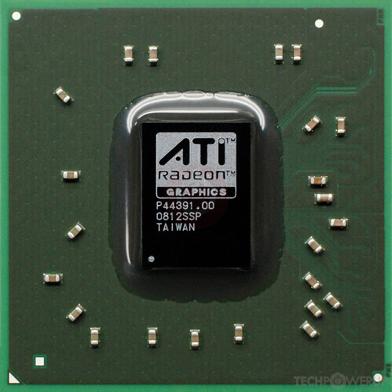
- Graphics Processor
- RV620
- Cores
- 40
- TMUs
- 4
- ROPs
- 4
- Memory Size
- 256 MB
- Memory Type
- DDR2
- Bus Width
- 64 bit

GPU
Graphics Processor
Graphics Card
- Release Date
- Dec 10th, 2007
- Generation
-
Radeon R600
(HD 3400)
- Predecessor
- Radeon R500 PCIe
- Successor
- Radeon R700
- Production
- End-of-life
- Bus Interface
- PCIe 2.0 x16
Clock Speeds
- GPU Clock
- 600 MHz
- Memory Clock
-
500 MHz
1000 Mbps effective
Memory
- Memory Size
- 256 MB
- Memory Type
- DDR2
- Memory Bus
- 64 bit
- Bandwidth
- 8.000 GB/s
Render Config
- Shading Units
- 40
- TMUs
- 4
- ROPs
- 4
- Compute Units
- 2
- L2 Cache
- 64 KB
Theoretical Performance
- Pixel Rate
- 2.400 GPixel/s
- Texture Rate
- 2.400 GTexel/s
- FP32 (float)
- 48.00 GFLOPS
Board Design
- Slot Width
- Single-slot
- TDP
- 25 W
- Suggested PSU
- 200 W
- Outputs
- 1x DVI
1x VGA
1x S-Video
- Power Connectors
- None
- Board Number
- B629
Graphics Features
- DirectX
- 10.1 (10_1)
- OpenGL
- 3.3
- OpenCL
- N/A
- Vulkan
- N/A
- Shader Model
- 4.1
Card Notes
| Variant Memory: 512 MB |
RV620 GPU Notes
| Mobile Variant: M82 / M84 Codename: Koopa Graphics/Compute: GFX3 Display Core Engine: 3.0 Unified Video Decoder: 1.0 |
Other retail boards based on this design (2)
| Name | GPU Clock | Memory Clock | Other Changes |
|---|---|---|---|
| 820 MHz | 700 MHz | 128 MB, GDDR3 | |
|
Sapphire HD 3450 HyperMemory

|
600 MHz | 500 MHz |

May 13th, 2024 08:59 EDT
change timezone
Latest GPU Drivers
New Forum Posts
- 5950X - Lowering SOC Voltage at 0.9 (0)
- Rare GPUs / Unreleased GPUs (1882)
- not impressed - nvme vs ssd (79)
- Dell Undervolting Lock Removed for 9th Gen Intel CPU (i7-9750h) (5)
- AIO Water Cooler vs Tower Air Cooler (14)
- 4K Gamers, How much VRAM do you have? (134)
- Purchased an AX1200i PSU as part of some forward planning, what tier is this PSU? (63)
- Cyberpunk 2077 Game Discussion (2127)
- Soundbar or 2.1 speaker for virtual 3d audio in PC games... (15)
- have LGA 1155 motherboard which xeon processor will fit ? (7)
Popular Reviews
- ZMF Caldera Closed Planar Magnetic Headphones Review
- Corsair MP700 Pro SE 4 TB Review
- Bykski CPU-XPR-C-I CPU Water Block Review - Amazing Value!
- ThundeRobot ML903 NearLink Review
- Upcoming Hardware Launches 2023 (Updated Feb 2024)
- CHERRY XTRFY M64 Pro Review
- AMD Ryzen 7 7800X3D Review - The Best Gaming CPU
- ASUS Radeon RX 7900 GRE TUF OC Review
- Corsair iCUE Link RX120 RGB 120 mm Fan Review
- Sapphire Radeon RX 7900 GRE Pulse Review
Controversial News Posts
- Intel Statement on Stability Issues: "Motherboard Makers to Blame" (266)
- AMD to Redesign Ray Tracing Hardware on RDNA 4 (224)
- Windows 11 Now Officially Adware as Microsoft Embeds Ads in the Start Menu (172)
- NVIDIA to Only Launch the Flagship GeForce RTX 5090 in 2024, Rest of the Series in 2025 (152)
- Sony PlayStation 5 Pro Specifications Confirmed, Console Arrives Before Holidays (119)
- AMD's RDNA 4 GPUs Could Stick with 18 Gbps GDDR6 Memory (114)
- AMD Hits Highest-Ever x86 CPU Market Share in Q1 2024 Across Desktop and Server (111)
- AMD Ryzen 9 7900X3D Now at a Mouth-watering $329 (104)