News Posts matching #20A

Return to Keyword Browsing

Report: Intel Seeks $2 Billion in Funding for Ireland Fab 34 Expansion

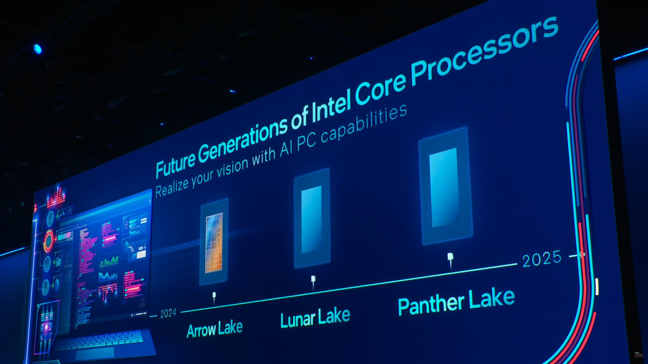
According to a Bloomberg report, Intel is seeking to raise at least $2 billion in equity funding from investors for expanding its fabrication facility in Leixlip, Ireland, known as Fab 34. The chipmaker has hired an advisor to find potential investors interested in providing capital for the project. Fab 34 is currently Intel's only chip plant in Europe that uses cutting-edge extreme ultraviolet (EUV) lithography. It produces processors on the Intel 4 process node, including compute tiles for Meteor Lake client CPUs and expected future Xeon data center chips. While $2 billion alone cannot finance the construction of an entirely new fab today, it can support meaningful expansion or upgrades of existing capacity. Intel likely aims to grow Fab 34's output and/or transition it to more advanced 3 nm-class technologies like Intel 3, Intel 20A, or Intel 18A.

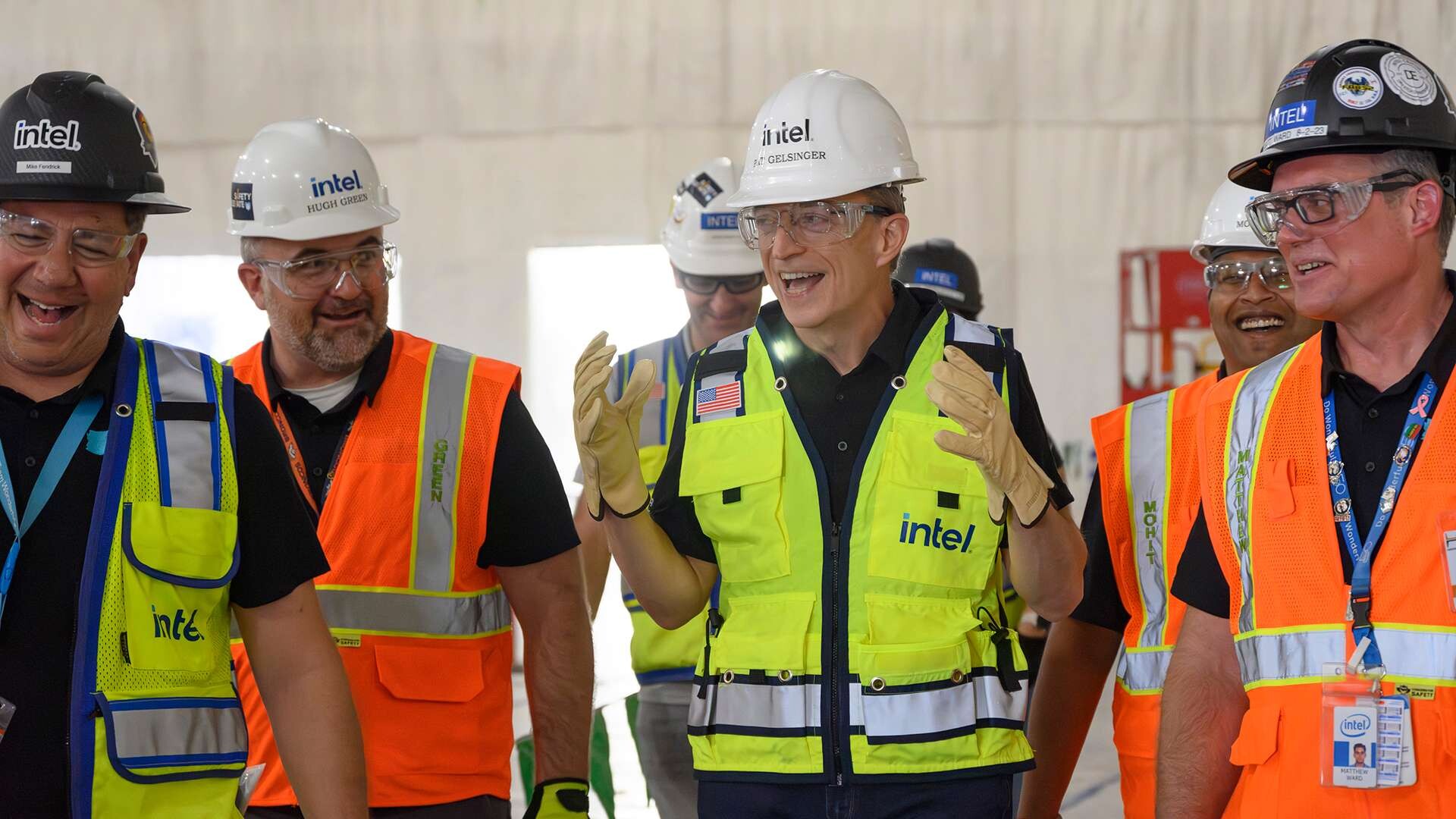
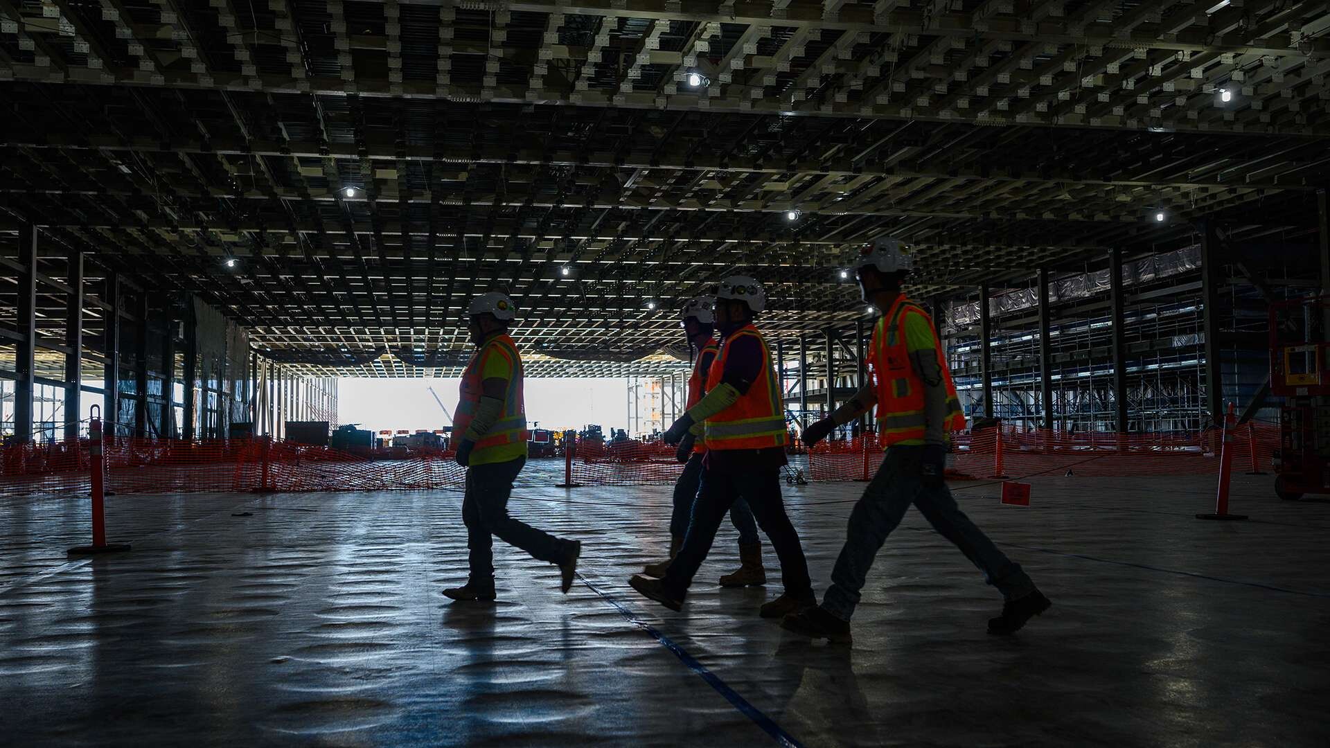
Expanding production aligns with Intel's needs for its own products and its Intel Foundry Services business, providing contract manufacturing. Intel previously secured a $15 billion investment from Brookfield Infrastructure for its Arizona fabs in exchange for a 49% stake, demonstrating the company's willingness to partner to raise capital for manufacturing projects. The Brookfield deal also set a precedent of using outside financing to supplement Intel's own spending budget. It provided $15 billion in effectively free cash flow Intel can redirect to other priorities like new fabs without increasing debt. Intel's latest fundraising efforts for the Ireland site follow a similar equity investment model that leverages outside capital to support its manufacturing expansion plans. Acquiring High-NA EUV machinery for manufacturing is costly, as these machines can reach up to $380 million alone.

Intel "Panther Lake" Targets Substantial AI Performance Leap in 2025

Pat Gelsinger, CEO of Intel Corporation, has outlined future performance expectations for the company's Core range of processors. In a recent fourth quarter 2023 earnings call he declared: "The Core Ultra platform delivers leadership AI performance today with our next-generation platforms launching later this year, Lunar Lake and Arrow Lake tripling our AI performance. In 2025 with Panther Lake, we will grow AI performance up to an additional 2x." Team Blue's Intel Core Ultra "Meteor Lake" mobile processors arrived right at the tail end of last year, as a somewhat delayed answer to AMD's Ryzen 7040 "Phoenix" APU series—both leveraging their own AI-crunching NPU technologies. Gelsinger believes that the launch of Lunar Lake and Arrow Lake Core product lines will bring significant (3x) AI processing improvements over Meteor Lake. He seemed to confident in a delay-free release schedule for the new year and beyond: "We are first in the industry to have incorporated both gate-all-around and backside power delivery in a single process node, the latter unexpected two years ahead of our competition. Arrow Lake, our lead Intel 20A vehicle will launch this year."

He proceeded to gush about their next node advancement: "Intel 18A is expected to achieve manufacturing readiness in second half 2024, completing our five nodes in four year journey and bringing us back to process leadership. I am pleased to say that Clearwater Forest, our first Intel 18A part for servers has already gone into fab and Panther Lake for clients will be heading into Fab shortly." Industry experts posit that Core "Panther Lake" parts could borrow elements from the next generation Xeon "Clearwater Forest" efficiency-focused family—possibly the latter's "Darkmont" E-cores, to accompany "Cougar Cove" P-cores. The Intel CEO is quite excited about the manufacturing outlay for 2025: "I'll just say, hey, we look at this every single day and we're scrutinizing carefully our progress on 18A. And obviously the great news that we just described those Clearwater Forest taping out, that gives us a lot of confidence that 18A is healthy. That's a major product for us. Panther Lake following that shortly."

Intel's Arizona Expansion Marks Construction Milestone

Marking a milestone in Intel's ongoing manufacturing expansion in Arizona, the company today announced that the initial portion of the cleanroom is "weather tight" and the "blow down" phase has begun at the company's two new leading-edge chip factories on its Ocotillo campus in Chandler, Arizona. This milestone underscores Intel's dedication to advancing its presence in the state and fostering technological innovation.

"Our commitment to Arizona runs deep, and as we expand our operations, we remain dedicated to addressing the growing demand for semiconductors and helping the United States regain its leadership position in this vital industry. This milestone represents the result of great teamwork, proficient teams and exceptional craftsmanship of the tradespeople, and it's thanks to their hard work that we've made such significant progress on our site while keeping our culture of caring and the safety of all as our top priority." -Dan Doron, Intel vice president and general manager of Fab Construction Enterprise

Intel LGA-1851 "Arrow Lake" Socket Detailed

Thanks to the 3D renders and technical drawings obtained by Igor's Lab, we have insights into the structure of Intel's next-generation LGA-1851 socket for Arrow Lake processors. Scheduled to arrive in mid-2024, the LGA-1851 socket was originally intended for Meteor Lake-S desktop processors. However, the socket is now awaiting Arrow Lake since Meteor Lake is now a mobile-only processor generation. The first notable thing about LGA-1851 is that it will directly connect a dedicated PCIe 5.0 x4 interface to the CPU, besides the x16 lanes going to the GPU. This results in native support for high-speed PCIe 5.0 NVMe SSDs that can achieve speeds of over 12 GB/s in both read and write workloads.

Intel Arrow Lake-S will be available with eight P-cores and 16 E-cores in SKUs with different combinations of the two. The accompanying 800 series chipset includes Z890, B860, and H810 models, with an evident absence of H870 SKU. There will be W880 and Q870 workstation-grade chipsets as well. It is worth pointing out that Arrow Lake will enable DRAM capacities of up to 48 GB per DIMM at 6400 MT/s. We expect to hear more about Arrow Lake-S as we near the 2024 launch date and we get to see the Intel 20A node being used in client products. Below, you can see the technical drawings of the Independent Loading Mechanism (ILM) and chipset 3D models.

Intel Arrow Lake-S to Feature 3 MB of L2 Cache per Performance Core

Intel's next-generation designs are nearing launch, and we are already getting information about the upcoming generations. Today, we have the information that Intel's Arrow Lake-S desktop/client implementations of the Arrow Lake family will feature as much as 3 MB of level two (L2) cache for each performance core. Currently, Intel's latest 13th-generation Raptor Lake and 14th-generation Raptor Lake Refresh feature 2 MB of L2 cache per performance core. However, the 15th generation Arrow Lake, scheduled for launch in 2024, will bump that up by 50% and reach 3 MB. Given that P-cores are getting a boost in capacity, we expect E-cores to do so as well, but at a smaller size.

Arrow Lake will utilize Lion Cove P-core microarchitecture, while the E-core design will be based on Skymont. Intel plans to use a 20A node for this CPU, and more details will be presented next year.

Intel, Ericsson Expand Collaboration to Advance Next-Gen Optimized 5G Infrastructure

Today, Intel announced a strategic collaboration agreement with Ericsson to utilize Intel's 18A process and manufacturing technology for Ericsson's future next-generation optimized 5G infrastructure. As part of the agreement, Intel will manufacture custom 5G SoCs (system-on-chip) for Ericsson to create highly differentiated leadership products for future 5G infrastructure. Additionally, the companies will expand their collaboration to optimize 4th Gen Intel Xeon Scalable processors with Intel vRAN Boost for Ericsson's Cloud RAN (radio access network) solutions to help communications service providers increase network capacity and energy efficiency while gaining greater flexibility and scalability.

"As our work together evolves, this is a significant milestone with Ericsson to partner broadly on their next-generation optimized 5G infrastructure. This agreement exemplifies our shared vision to innovate and transform network connectivity, and it reinforces the growing customer confidence in our process and manufacturing technology," said Sachin Katti, senior vice president and general manager of the Network and Edge group at Intel. "We look forward to working together with Ericsson, an industry leader, to build networks that are open, reliable and ready for the future."

Intel to Demonstrate PowerVia on E-Core Processor Built with Intel 4 Node

At VLSI Symposium 2023, scheduled to take place between June 11-16, Intel is set to demonstrate its PowerVia technology working efficiently on an E-Core chip built using the Intel 4 node. Conventional chips have power and signal interconnects distributed across multiple metal layers. PowerVia, on the other hand, dedicates specific layers for power delivery, effectively separating them from the signal routing layers. This approach allows for vertical power delivery through a set of power-specific Through-Silicon Vias (TSVs) or PowerVias, which are essentially vertical connections between the top and bottom surfaces of the chip. By delivering power directly from the backside of the chip, PowerVia reduces power supply noise and resistive losses, optimizing power distribution and improving overall energy efficiency. PowerVia is set to make a debut in 2024 with Intel 20A node.

For VLSI Symposium 2023 talk, the company has prepared a paper that highlights a design made using Intel 4 technology and implements E-Cores only in a test chip. The document states: "PowerVia Technology is a novel innovation to extend Process Scaling by having Power Delivery on the backside. This paper presents the pre and post silicon findings from implementing an Intel E-Core in PowerVia Technology. PowerVia enabled standard cell utilization of greater than 90 percent in large areas of the core while showing greater than 5 percent frequency benefit in silicon due reduced IR drop. Successful Post silicon debug is demonstrated with slightly higher but acceptable throughput times. The thermal characteristics of the PowerVia testchip is inline with higher power densities expected from logic scaling."

Intel 20A and 18A Foundry Nodes Complete Development Phase, On Track for 2024 Manufacturing

Intel Foundry Services, the in-house semiconductor foundry of Intel, announced that its 2 nm-class Intel 20A and 1.8 nm-class Intel 18A foundry nodes have completed development, and are on course for mass-producing chips on their roadmap dates. Chips are expected to begin mass-production on the Intel 20A node in the first half of 2024, while those on the Intel 18A node are expected to begin in the second half of 2024. The completion of the development phase means that Intel has finalized the specifications and performance/power targets of the nodes, the tools and software required to make the chips, and can now begin ordering them to build the nodes. Intel has been testing these nodes through 2022, and with the specs being finalized, chip-designers can accordingly wrap up development of their products to align with what these nodes have to offer.

Intel 20A (or 20-angstrom, or 2 nm) node introduces gates-all-around (GAA) RibbonFET transistors with PowerVIAs (an interconnect innovation that contributes to transistor densities). The Intel 20A node is claimed to offer a 15% performance/Watt gain over its predecessor, the Intel 3 node (FinFET EUV, 3 nm-class), which by itself offers an 18% performance/Watt gain over Intel 4 (20% perf/Watt gain over the current Intel 7 node), the node that is entering mass-production very soon. The Intel 18A node is a further refinement of Intel 20A, and introduces a design improvement to the RibbonFET that increases transistor density at scale, and a claimed 10% performance/Watt improvement over Intel 20A.

Intel Foundry Services Allegedly Working on Test Chips for 43 Potential Customers

A new story is making the rounds, citing Wang Rui, chair Intel China, in the media in both China and Taiwan, claiming that Intel is working on test chips for as many as 43 potential customers for Intel Foundry Services (IFS). At least seven of those potential customers are said to be from the top 10 foundry clients globally. This sounds a bit too good to be true, considering that IFS has as yet to prove that they can deliver on their promises.

Furthermore, Wang Rui is meant to have gone on record, saying that IFS has taped out products on both its 20A and 18A nodes. Exactly what these products are, wasn't divulged, but as the 18A node isn't expected to go into mass production until the second half of 2024, this sounds a little bit too good to be true. What makes this even less believable is that the Intel 4 node is only set to go into mass production in the second half this year and before Intel moves to its Ångström nodes, the company still has to deliver on its Intel 3 node. The Intel China chair is also reportedly confident that Intel will be returning to a leading foundry position by 2025.
Return to Keyword Browsing
Apr 29th, 2024 19:28 EDT change timezone

New Forum Posts

Popular Reviews

Controversial News Posts