News Posts matching #40nm

Return to Keyword Browsing

NVIDIA Likely to Start 40nm GPU Conquest with GT218

As the industry moves closer to implementation of the 40nm silicon technology on graphics processors, some of the most complex electronic devices, both AMD and NVIDIA have their offerings in the works. While AMD already has prototypes taped out, NVIDIA seems to be taking its time, perhaps to perfect its products.

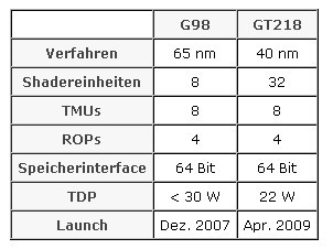
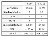
The green camp, as Hardware-Infos finds out, is likely to start its 40nm lineup with the GT218 graphics processor. With NVIDIA's internal coding scheme, the GT218 is an entry-level GPU. In its generation hierarchy, would be the GT215, GT216 (mainstream) and GT212 (high-end). The GT218 will succeed the G98 GPU that went into making the GeForce 9300 series. It will have 32 stream processors, 8 texture memory units, and 4 raster operations pipelines. It will continue to have a 64-bit wide memory bus. Despite the increase in transistor counts, the GPU ends up with a lower TDP, expected to be around 22W, as against the roughly 30W for the G98. The GT218 is slated for April, later this year.

RV790 Samples Carry Faster Memory

Having taped out late last year, samples based on the new RV790 graphics processor have been doing rounds in the industry. A few more details have surfaced about it. Earlier noted to have identical clock speeds to that of the RV770XT (Radeon HD 4870), the RV790 samples are now known to have higher memory clock speeds. While the Radeon HD 4870 has its memory frequency at 900 MHz GDDR5 (effective 3.60 GHz), the samples carry memory clocked at 975 MHz (effective 3.90 GHz). Interestingly the memory chips on the sample, labeled IDGV1G-05A1F1C-40X, made by Qimonda, are specified to run at 1.00 GHz, reaching the 4 GHz effective memory speed mark. The samples feature 1 GB of memory. The RV790 is AMD's new current-generation graphics processor built on the newer 40nm silicon fabrication process. The new process is expected to reduce the GPU's power consumption and thermal footprint. The RV790 is conceived to be an immediate successor to the RV770 GPU.

GT300 A Leap Forward for NVIDIA GPU Architecture

Every once in a while, comes a GPU by NVIDIA that marks the evolution of GPU architecture for NVIDIA. A good example of this would be the G80, which was a distinct evolution of the GPU architecture for the company. Sources tell Hardware-Infos that the GT300 is on course of being one such GPU that comes with distinct architectural changes. To begin with, GT300 will start the company's DirectX 11 conquest the way its ancestor, the G80 did for DirectX 10, which turned out to be largely a successful one.

The GT300's architecture will be based on a new form of number-crunching machinery. While today's NVIDIA GPUs feature a SIMD (single instruction multiple data) computation mechanism, the GT300 will introduce the GPU to MIMD (multiple instructions multiple data) mechanism. This is expected to boost the computational efficiency of the GPU many-fold. The ALU cluster organization will be dynamic, pooled, and driven by a crossbar switch. Once again, NVIDIA gets to drop clock-speeds and power consumptions, while achieving greater levels of performance than current-generation GPUs. With GT300, NVIDIA will introduce the next major update to CUDA. With the new GPUs being built on the 40nm silicon fabrication process, transistor counts are expected to spiral-up. NVIDIA's GT300 is expected to go to office in Q4 2009, with its launch schedule more or less dependent on that of Microsoft's Windows 7 operating system that brings in DirectX 11 support.

More GT212 Information Forthcoming

NVIDIA's G200b, its current flagship GPU will be suceeded later this year with the GT212, and as Hardware Infos discovers, NVIDIA seems to have given some interesting specifications to the GT212. To begin with, the GPU holds more than 1.8 billion transistors. It is built on TSMC's 40nm manufacturing node. The shader domain gets a boost with 384 shader units (a 60% increase over G200(b)). The GPU holds 96 texture memory units and a 256-bit wide GDDR5 memory bus with a clock speed of 1250 MHz (5000 MT/s).

The transition to GDDR5 seemed inevitable, with there being a genuine incentive of cutting down the number of memory chips (due to the efficient memory bus), with NVIDIA having completely avoided GDDR4. With the die-size being expected to be around 300 sq. mm, these GPUs will be cheaper to manufacture. The GT212 is slated for Q2 2009.

The Foundry Company to Make GPUs, To Accept Designs from Other Manufacturers Soon

At the AMD Analyst Day event, AMD indicated in its presentations that The Foundry Company, a manufacturing company formed from the assets of AMD with the intestments of ATIC under the AssetSmart program, would in the future become an independent foundry company accepting foundry partnerships from companies apart from its one largest customer, AMD. The move would keep the newly formed company profitable and competitive with other Asian foundry companies.

In the same presentation, AMD also indicated that eventually it would assign manufacturing of its ATI Radeon GPUs and chipsets, to The Foundry Company (TFC). Currently GPUs and chipsets are being manufacuted by foundry companies such as TSMC and UMC in Taiwan. This move would send a significant chunk of manufacturing to TFC. Sources tell ATI Forum.de that at FAB38 Dresden, a major manufacturing facility, installations of the 40nm bulk manufacturing node is in full-swing (not to be confused with 45nm SOI, on which K10.5 processors are built). Also there are indications of the facility accepting orders for manufacturing chips on the new node from other fab-less companies, an attempt to bring in profitability right from the start.

VIA Preparing Dual-Core Nano 3000 Processor for H2 2009

VIA, the third active player in the x86 processor market, is known for its low-power processors catering to the ULPC segment of the market. Sources tell HKEPC that the firm is now readying a dual-core variant of its Intel Atom competitor, the Nano 3000. The Nano 3000 series, slated for launches throughout 2009 includes a new architecture by VIA, while bearing the same essential Nano-BGA package.

The processor would use a boarder system interface with the 1333 MHz VIA V4 bus (FSB). It will feature x86-64 extension along with the SSE4 instruction sets to make it standards compliant. It will feature 128KB of L1 and 1MB of L2 caches. VIA is also looking to improve the processor's number-crunching capabilities by working on its integer and floating-point operations efficiency. The processor will be built on the Japanese Fujitsu 65nm manufacturing process which has so far been VIA's foundry partner with processors and S3 Graphics products. The company is also considering a switch to the TSMC 40nm or 45nm node later, sources note. The VIA Nano 3000 Dual-Core variant can be expected in the second-half of 2009, while single core variants of the architecture can be expected earlier.

NVIDIA GPU Lineup for 2009 Tabled

The year 2008 has been eventful for the PC graphics industry. This is the year which, for the most of the part, saw some serious competition between NVIDIA and ATI. While pure horsepower and value are what determined product superiority, implementing new technologies is what looks to drive GPU makers in 2009. One of the first of these technologies is the introduction of the 40nm manufacturing process, which facilitates GPU makers to step-up transistor counts or even cut manufacturing costs. VR-Zone, based on a few documents it has access to, compiled a list of GPUs that NVIDIA could pull out of its hat in 2009.

To begin with, NVIDIA is expected to have a full-fledged lineup of GPUs top-to-bottom built on the 40nm fab process within 2009. Before it makes the move to the new fab process, the G200b, built on the 55nm fab process will be given a chance to hold the performance and enthusiast segment offerings by the company, in Q1. Come Q2, and the G200b will be succeeded by GT212. All that while, current G94, G96, G98 will hold the mainstream thru value segments, only to be replaced by GT214, GT216 and GT218 respectively in Q3. NVIDIA's gets a newer IGP too, the iGT209. NVIDIA looks to end the year with a newer high-end GPU, the GT300 to succeed GT212 in Q4.

NVIDIA GT216 Specifications Trickle-In

The AMD RV740 has been gaining quite some attention lately. Following news of it being the first GPU to be built on the 40nm manufacturing process, there is some information trickling in about NVIDIA's offering to combat it. The GT216, unlike what most speculations talked about being a next generation high-end GPU, is supposed to be a mainstream GPU whose specifications make it a rival to the AMD RV740. This, according to specifications of the said GPU emerging from Beyond3D, part of which they are sure of, part speculation.

For starters, the GT216 will be built on the 40nm manufacturing process. It will feature a 192-bit wide GDDR3 memory bus. Graphics cards built on this would feature 768 MB of memory (with possible OEM variants having just 384 MB). The memory is clocked at 1200 MHz (2400 MHz DDR). There is speculation linked to the rest of the specs at this point in time, notably that it might have 7 ALU clusters (168 SPs). The manufacturing process will make sure the GPU is cost-effective. With this, the next round of mainstream GPU competition sounds even more exciting.

RV740 Successfully Taped Out, Other 40nm GPUs Follow

The RV740 graphics processor by AMD could well be the first GPU in production, to be built on the newer 40nm manufacturing process, giving its makers something to brag about. The RV740 design and specifications are largely derived from the RV770LE (covered here), while bringing the GDDR5 memory standard to the mainstream.

Chinese industrial journals tell DigiTimes that the company has completed taping-out the RV740, and that the GPU is awaiting mass-production by AMD's foundry partner, Taiwan Semiconductor Manufacturing Company (TSMC). Mass production of products based on this GPU could commence by the end of Q1 2009.

RV740 a 40nm RV770LE in Disguise?

RV740, the first GPU built by AMD on the 40nm silicon fabrication process, seems to be gaining attention. While earlier reports suggested this core to be simply a miniaturized RV730, a fresh report emerging from VR-Zone says otherwise.

The RV740 is supposed to be largely derived from the RV770, as in its RV770LE avatar which went into making the ATI Radeon HD 4830. There are some interesting specifications attached to it. To begin with, the core physically holds only 640 stream processors, in comparison to the 800(+) on the RV770. The core continues to have 32 texture memory units (TMUs) and 16 render back-ends. Interestingly, there is a 128-bit wide GDDR5 memory bus instead of 256-bit wide GDDR3 (for the RV770LE). With this, the RV740 has a rated memory bandwidth identical to that of the RV770LE, 57.6 GB/s, though the bus width would warrant the use of lesser number of memory chips, and effectively reduce manufacturing costs. Graphics cards based on this GPU are expected to emerge in early 2009. You can also expect derivatives based on this core with GDDR4, GDDR3 or even DDR2 memory. In any case, the products are expected to cost below US $100.

RV740 Taped-Out, First 40nm GPU From AMD

The manufacturing process technologies for graphics processors that dominated the 2008 were TSMC 65nm and 55nm. While AMD made the transition to 55nm over an year ago, it was a little later when we started seeing 55nm versions of existing NVIDIA GPUs.

A month into TSMC's announcement of of its 40nm bulk production node, AMD has reportedly taped out its first 40nm GPU, the RV740. While this is no high-end GPU, it is supposed to be the first successful port of AMD's GPU architecture to the new node. The RV740 succeeds the RV730, the GPU that went into the making the Radeon HD 4670. It is a mainstream GPU that ideally should make it to the sub-$100 graphics card segment. With RV740, AMD gains some experience as a manufacturer as it works on the RV870 "Lil' Dragon", the next generation GPU from the red camp. A product based on the RV740 can be expected only after Q1 2009.

Hynix 7GT/s GDDR5 Chip to Make it to Major SKUs, R700 Included

Sources in the industry point out that the 7 GT/s GDDR5 memory chip made by Hynix (model: H5GQ1H24AFR), which was announced earlier in this week, would make it to several major graphics board SKUs by both AMD and NVIDIA. The two companies have chosen TSMC and its 40nm fabrication process as the foundry partner for their upcoming 40nm graphics processors, namely AMD RV870 and NVIDIA GT212.

Both these chips would feature GDDR5 memory bus capabilities, and there are indications of the 7 GT/s DRAM chip being incorporated into graphics boards based on these GPUs. Additionally, there is also word that AMD will be using the said DRAM chip in its current flagship graphics card, the Radeon HD 4870 X2 in the near future. Both AMD and NVIDIA are expected to have taped out their 40nm GPU designs within Q1, 2009.

Taiwan Semiconductor Manufacturing Company (TSMC) Announces 40nm Volume Production

Taiwan Semiconductor Manufacturing Company (TSMC) today announced volume production of the first semiconductor foundry 40nm logic manufacturing process with the successful ramp of its 40 nanometer (nm) General Purpose (G) and Low Power (LP) versions. Nanometers measure the width of metal lines in semiconductors. Forty nanometers is less than one-thousandth the width of a human hair.
The 40nm process is one of the semiconductor industry's most advanced available for production manufacturing process and is expected to play a key role in the development of next generation products in global consumer electronics, mobile, and computer end markets.

AMD to Give RV770 a Refresh, G200b Counterattack Planned

The RV770 graphics processor changed AMD's fortunes in the graphics processor industry and put it back in the race for supremacy over the larger rival NVIDIA. The introduction of RV770-based products had a huge impact on the mid-range and high-end graphics card markets, which took NVIDIA by surprise. Jen-Hsun Huang, the CEO of NVIDIA has been quoted saying that they had underestimated their competitor's latest GPU, referring to RV770. While the Radeon HD 4870 graphics accelerator provided direct competition to the 192 shader-laden GeForce GTX 260, the subsequent introduction of a 216 shader variant saw it lose ground, leaving doubling of memory size to carve out the newer SKU, the Radeon HD 4870 1GB. Performance benchmarks of this card from all over the media have been mixed, but show that AMD isn't giving up this chance for gaining technological supremacy.

In Q4 2008, NVIDIA is expected to release three new graphics cards: GeForce GTX 270 and GeForce GTX 290. The cards are based on NVIDIA's G200 refresh, the G200b, which incorporates a new manufacturing technology to facilitate higher clock-speeds, stepping up performance. This looks to threaten the market position of AMD's RV770, since it's already established that G200 when overclocked to its stable limits, achieves more performance than RV770 pushed to its limits. This leaves AMD with some worries, since it cannot afford to lose the wonderful market-position its cash-cow, the RV770 is currently in, to an NVIDIA product that outperforms it by a significant margin, in its price-domain. The company's next generation graphics processor would be the RV870, which still has some time left before it could be rushed in, since its introduction is tied to the constraints of foundry companies such as TSMC, and the availability of the required manufacturing process (40nm silicon lithography) by them. While TSMC takes its time working on that, there's a fair bit of time left, for RV770 to face NVIDIA, which given the circumstances, looks a lost battle. Is AMD going to do something about its flagship GPU? Will AMD make an effort to maintain its competitiveness before the next round of the battle for technological supremacy begins? The answer is tilting in favour of yes.

Power and Innovation to Drive High-End GPUs in 2009

The year 2008 so far, has been very eventful for the graphics card market. A reinvigorated GPU lineup by ATI, brought in some fierce competition to NVIDIA, which resulted in a tug-of-war with pricing graphics cards in the market, with either company refusing to lose on grounds of pricing. This event, coupled with the announcement of several game titles by game publishers, resulted in bumper-sales of graphics cards, giving the present state of the global economy little or no relevance.

The months to come hold the same amount of importance for both AMD and NVIDIA, where the next round of competition begins with successors to current high-end products being slated. NVIDIA is expected to continue with its monolithic high transistor-count GPU design methodology, while AMD could bring in a little change to the way it uses two efficient GPUs to build powerful products.

NVIDIA and AMD to begin 40nm GPU Conquests in 2009

Reports suggest that the Taiwan Semiconductor Manufacturing Company (TSMC) could receive manufacturing contracts by AMD, and long-time customer NVIDIA, for graphics processors based on the newest 40nm silicon fabrication process. The two giants in the visual computing industry, are expected to skip the 45nm process altogether. This is seen as a move to cut down manufacturing costs, and use the most feasible manufacturing technologies. Miniaturizing circuitry at that scale would allow them to build even more complex silicon machinery, with much higher transistor counts, while maintaining size constraints.

AMD on its part would have to use the services of TSMC, since the foundry company's fab in Dresden is only capable of 45nm SOI fabrication process, and that it would take as long as 2010, by the time the expected 32nm process is ready at the New York fab. The next star-entry for AMD would be the ATI RV870, and as for NVIDIA, it would continue development of monolithic high-end GPUs with GT216, a successor to the G200 GPU. Meanwhile, the companies could continue aggressive competition, with projections of up to 20% price-cuts by Christmas 2008 shopping season. Their 40nm GPU designs could be ready by the end of this year, and 40nm GPUs could be supplied by June, 2009.

AMD Slates 40/45nm GPUs for Early-2009, RV870 on the Cards

As we inch closer to the R700 release, which previews prove to have dethroned the GeForce GTX 280 convincingly, taking the crown for the fastest graphics card there is, NordicHardware reports AMD could be giving 'final-touches' to a fresh-wave of GPUs for early 2009. The timing is a critical factor here as that's the time-range the proposed NVIDIA G300 carrying 384 SP's and 512bit GDDR5 memory bus is marked for. The R800 cards could carry 2,000 stream processors, with its unit processors the RV870 holding 1,000 stream processors each. They could enter the realm of either 40nm or 45nm fabrication process.

TSMC Readies 40nm Semiconductor Manufacturing Process

Taiwan Semiconductor Manufacturing Company (TSMC) recently unveiled the foundry's first 40 nanometer (nm) manufacturing process technology. The new node supports a performance-driven general purpose (40G) technology and a power-efficient low power (40LP) technology. It features a full design service package and a design ecosystem that covers verified third party IP, third party EDA tools, TSMC-generated SPICE models and foundation IPs. First wafers out are expected in the second quarter of 2008.
Return to Keyword Browsing
May 4th, 2024 17:43 EDT change timezone

New Forum Posts

Popular Reviews

Controversial News Posts