News Posts matching #7nm

Return to Keyword Browsing

AMD Navi Found Secretly Hiding in Linux Drivers

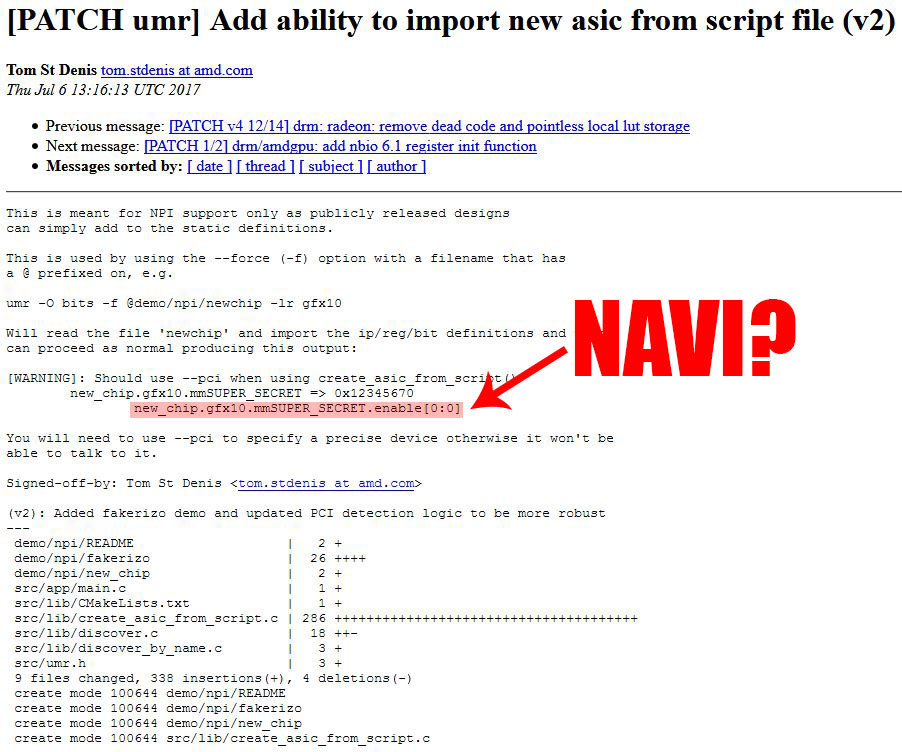
We know AMD has been doing a great job keeping the lid on their Navi architecture with information being scarce at the moment. Aside from knowing that Navi is being fabricated on the 7 nm process, it is possible that the microarchitecture will quite possibly support next-generation memory like GDDR6 or HBM3. In a Navi discussion on the Beyond3D forums, a user found an entry in a Linux driver dated back to July that apparently mentions AMD's upcoming architecture - not by its real name, of course. The code is to add support for importing new asic definitions from a text file as opposed to adding support in code. Tom St Denis, a software engineer at AMD, listed the output that would be generated by using this functionality. However, the entry that caught our attention reads: new_chip.gfx10.mmSUPER_SECRET.enable [0: 0]. If our memory serves us right, the codename for Vega was GFX9. So by logic, Navi should carry the GFX10 codename. Obviously, the SUPER_SECRET part further backs up our theory or maybe AMD's just trolling us. The red team has been hiring personnel for their GFX10 projects, so we can assume they're working diligently to release Navi some time next year.

Samsung Announces 11nm LPP and 7nm LPP With EUV Technology

Samsung Electronics Co., Ltd., the world leader in advanced semiconductor technology, today announced it has added 11-nanometer (nm) FinFET process technology (11LPP, Low Power Plus) to its advanced foundry process portfolio, offering customers with an even wider range of options for their next-generation products. Through further scaling from the earlier 14LPP process, 11LPP delivers up to 15 percent higher performance and up to 10 percent chip area reduction with the same power consumption.

In addition to the 10nm FinFET process for mobile processors in premium flagship smartphones, the company expects its 11nm process to bring differentiated value to mid- to high-end smartphones. The new process technology is scheduled to be ready for production in the first half of 2018. Samsung also confirmed that development of 7LPP with EUV (extreme ultra violet) lithography technology is on schedule, targeting its initial production in the second half of 2018.

Since 2014, Samsung has processed close to 200,000 wafers with EUV lithography technology and, building on its experience, has recently seen visible results in process development such as achieving 80 percent yield for 256 megabit (Mb) SRAM (static random-access memory).

GLOBALFOUNDRIES on Track to Deliver Leading-Performance 7nm FinFET Technology

GLOBALFOUNDRIES today announced the availability of its 7nm Leading-Performance (7LP) FinFET semiconductor technology, delivering a 40 percent generational performance boost to meet the needs of applications such as premium mobile processors, cloud servers and networking infrastructure. Design kits are available now, and the first customer products based on 7LP are expected to launch in the first half of 2018, with volume production ramping in the second half of 2018.

In September 2016, GF announced plans to develop its own 7nm FinFET technology leveraging the company's unmatched heritage of manufacturing high-performance chips. Thanks to additional improvements at both the transistor and process levels, the 7LP technology is exceeding initial performance targets and expected to deliver greater than 40 percent more processing power and twice the area scaling than the previous 14nm FinFET technology. The technology is now ready for customer designs at the company's leading-edge Fab 8 facility in Saratoga County, N.Y.

"Our 7nm FinFET technology development is on track and we are seeing strong customer traction, with multiple product tapeouts planned in 2018," said Gregg Bartlett, senior vice president of the CMOS Business Unit at GF. "And, while driving to commercialize 7nm, we are actively developing next-generation technologies at 5nm and beyond to ensure our customers have access to a world-class roadmap at the leading edge."

Samsung Details New Foundry Offerings at 14nm (LPU) and 10nm (LPU)

In an announcement that's sure to stir the foundry gods, Samsung Electronics, a world leader in advanced semiconductor technology, announced today that it is expanding its advanced foundry process technology offerings with the fourth-generation 14-nanometer (nm) process (14LPU) and the third-generation 10nm process (10LPU). The announcement comes as Samsung increases investment so as to meet the requirements of next generation products, ranging from mobile and consumer electronics (Snapdragon 830 and Samsung's own Exynos 8895 come to mind) to data centers and automotives.

Ben Suh, Senior Vice President of foundry marketing at Samsung Electronics, issued the following statement: "After we announced the industry's first 10nm mass production in mid-October, we have now also expanded our lineup with new foundry offerings, 14LPU and 10LPU. Samsung is very confident with our technology definitions that provide design advantages on an aggressive process with manufacturability considerations. We have received tremendous positive market feedback and are looking forward to expanding our leadership in the advanced process technology space."
Return to Keyword Browsing
Jun 12th, 2024 13:05 EDT change timezone

New Forum Posts

Popular Reviews

Controversial News Posts