News Posts matching #Cell

Return to Keyword Browsing

Samsung to Detail SF4X Process for High-Performance Chips

Samsung has invested heavily in semiconductor manufacturing technology to provide clients with a viable alternative to TSMC and its portfolio of nodes spanning anything from mobile to high-performance computing (HPC) applications. Today, we have information that Samsung will present its SF4X node to the public in this year's VLSI Symposium. Previously known as a 4HPC node, it is designed as a 4 nm-class node with a specialized use case for HPC processors, in contrast to the standard SF4 (4LPP) node that uses 4 nm transistors designed for low-power standards applicable to mobile/laptop space. According to the VLSI Symposium schedule, Samsung is set to present more info about the paper titled "Highly Reliable/Manufacturable 4nm FinFET Platform Technology (SF4X) for HPC Application with Dual-CPP/HP-HD Standard Cells."

As the brief introduction notes, "In this paper, the most upgraded 4nm (SF4X) ensuring HPC application was successfully demonstrated. Key features are (1) Significant performance +10% boosting with Power -23% reduction via advanced SD stress engineering, Transistor level DTCO (T-DTCO) and [middle-of-line] MOL scheme, (2) New HPC options: Ultra-Low-Vt device (ULVT), high speed SRAM and high Vdd operation guarantee with a newly developed MOL scheme. SF4X enhancement has been proved by a product to bring CPU Vmin reduction -60mV / IDDQ -10% variation reduction together with improved SRAM process margin. Moreover, to secure high Vdd operation, Contact-Gate breakdown voltage is improved by >1V without Performance degradation. This SF4X technology provides a tremendous performance benefits for various applications in a wide operation range." While we have no information on the reference for these claims, we suspect it is likely the regular SF4 node. More performance figures and an in-depth look will be available on Thursday, June 15, at Technology Session 16 at the symposium.

Winbond Introduces new Sequential Read Function in High-Speed QspiNAND Flash

Winbond Electronics Corporation, a leading global supplier of semiconductor memory solutions, today extended its record of leading the industry's innovation in specialty Flash memory with the introduction of a more flexible, high-speed read capability in its latest QspiNAND Flash products. Automotive and IoT device manufacturers are increasingly adopting high-performance Single-Level Cell (SLC) NAND Flash as a low-cost alternative at densities of 512 Mbits and higher to the NOR Flash traditionally used for code storage. Previous Winbond innovations in high-performance NAND Flash include the Quad SPI-NAND interface, which shares the same 6-pin signals and QSPI command set as Quad SPI-NOR, and the Continuous Read function, which achieves up to a 52 MB/s continuous data transfer rate at a 104 MHz clock frequency.

Phison Demonstrates 4-Bits Per Cell QLC SSDs

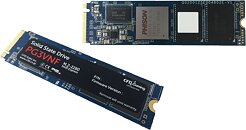
Phison Electronics, the industry's leader in flash controller and NAND storage solutions, is demonstrating mainstream performance using 4-bits per cell QLC NAND flash controllers and SSDs at the Consumer Electronics Show 2020 (CES) in Las Vegas, Nevada. In its private suite, Phison is showcasing the addition of support for QLC NAND to its already shipping E16 PCIe Gen 4x4, E12 PCIe Gen 3x4, and S12 SATA controllers that use TLC NAND. Phison's industry leading approach leverages highly successful controllers that were qualified by tier-1 OEMs, are in mass production now, and extends new SSD designs to utilize either TLC or QLC NAND. Phison's proprietary QLC NAND controller technology enables higher SSD capacities in industry standard form factors while meeting the performance demands of mainstream applications.

Phison's flagship E16 series controller for PCIe Gen 4x4 NVMe SSDs can achieve up to 4 TB in capacity with QLC NAND and reaches speeds of 4.9 GB/s for sequential reads and 3.8 GB/s for sequential writes. The E12 series controller enables PCIe Gen 3x4 NVMe SSDs and has a capacity of up to 8 TB and speeds of 3.4 GB/s sequential reads, 3.0 GB/s sequential writes with QLC NAND. For the SATA interface, Phison is also demonstrating the S12 controller series SSDs with up to 16 TB using QLC NAND and performance at 550 MB/s sequential reads and 530 MB/s sequential writes. Phison's DRAM-less S13T controllers enable smaller form factors, have a capacity of up to 2 TB, and operate at 550 MB/s sequential reads and 500 MB/s sequential writes.

Kioxia Develops New 3D Semicircular Flash Memory Cell Structure "Twin BiCS FLASH"

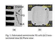
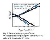
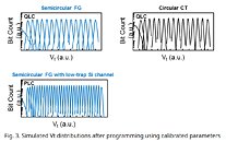
Kioxia Corporation today announced the development of the world's first three-dimensional (3D) semicircular split-gate flash memory cell structure "Twin BiCS FLASH" using specially designed semicircular Floating Gate (FG) cells. Twin BiCS FLASH achieves superior program slope and a larger program/erase window at a much smaller cell size compared to conventional circular Charge Trap (CT) cells. These attributes make this new cell design a promising candidate to surpass four bits per cell (QLC) for significantly higher memory density and fewer stacking layers. This technology was announced at the IEEE International Electron Devices Meeting (IEDM) held in San Francisco, CA on December 11th.

3D flash memory technology has achieved high bit density with low cost per bit by increasing the number of cell stacked layers as well as by implementing multilayer stack deposition and high aspect ratio etching. In recent years, as the number of cell layers exceeds 100, managing the trade-offs among etch profile control, size uniformity and productivity is becoming increasingly challenging. To overcome this problem, Kioxia developed a new semicircular cell design by splitting the gate electrode in the conventional circular cell to reduce cell size compared to the conventional circular cell, enabling higher-density memory at a lower number of cell layers.

Creative ZiiLabs Announces 100 Core CPU

ZiiLABS, a pioneering media processor and platforms company (a wholly-owned subsidiary of Creative Technology Ltd), today unveiled its ground-breaking 100-core ZMS-40 StemCell Media processor optimized for Android. The ZMS-40 combines 96 of ZiiLABS' StemCell media processing cores with four 1.5GHz ARM Cortex-A9 CPUs to deliver stunning multi-tasking application and media processing performance.

By doubling the number of StemCell Media processors compared to the previous ZMS-20, the ZMS-40 delivers twice the peak media performance, while running the larger array at lower clock speeds to achieve the same performance leads to greater energy efficiency and a reduction in power consumption of up to 50 percent. With 2X the performance and 2X the power efficiency, the ZMS-40 delivers ground-breaking media capabilities to handheld devices such as tablets, including ultra-high-resolution H.264 HP decoding of up to 3840x1080 for true 1080p 3D stereo, a rich and interactive desktop browsing experience, 2560x1600 (WQXGA) display resolution support, higher-quality video encoding and immersive OpenGL ES graphics and future support for High Efficiency Video Coding (HEVC).

OCZ Technology Unveils Indilinx Everest Series Solid State Drive Controller

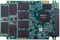
OCZ Technology Group, Inc., a leading provider of high-performance solid-state drives (SSDs) for computing devices and systems, today unveiled the Indilinx Everest SATA 3.0 SSD platform. The Everest platform features support of 6Gbps interface speeds, high transactional performance that is optimized for compressed files, and maximum capacities up to 1TB.

"The new Indilinx Everest platform is a complete customizable solution that delivers superior storage performance, features, and capabilities designed to exceed the needs of the most demanding SSD applications," said Bumsoo Kim, President of Indilinx. "Combining a 6Gbps SATA Revision 3.0 host interface, a dual-core CPU, and support for the latest, most advanced NAND Flash memory technology available, Everest offers SSD manufacturers unparallel flexibility in optimizing their designs for both performance and cost."

SpursEngine based Video Cards out Soon

The term "SpursEngine" might be a little new for some of us. It is the HD video processor Toshiba used in its Qosmio G55 and F40 high-end media notebooks, where the company chose to call it "Toshiba Quad-Core HD processor". The SpursEngine tag comes in, where the processor uses Toshiba's proprietary technology to accelerate graphics and HD video across multiple heads. The chip itself is derived from the CELL Broadband Engine (CBE), the central processor that drives the Sony Playstation 3 gaming console. Toshiba made modifications to the design, by reducing the number of synergistic processing elements (dubbed cores) to 4, with the common PowerPC thread arbiter remaining. It is specialized for video processing.

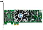
Toshiba has already formed collaborations with Leadtek and Thomson, the two companies would be the first to come out with cards based on this infant video processor. As such, these are not stand-alone video-cards as of now (they lack output logic), they stand to demonstrate the GPUs design methodology in a PC environment, so the companies could gain foothold. The cards could serve as HD video processing solutions, for industrial, office or home use. Toshiba could put in its proprietary video processing technologies into this product. The Leadtek Winfast PxVC 1100 is pictured below. It uses PCI-Express x1 interface, and comes with 128 MB of XDR memory. The cards could be out by the end of this month, and could carry a steep price-tag of US $286, at least going by the listings in Japan.

Toshiba's Newest Notebooks to Feature Modified CELL Processor

The first thing that comes to your mind when you talk about CELL Broadband Engine is probably the Sony Playstation 3. Toshiba, a prominent player in ultra-portable computing have announced that a new pair of laptops, the Qosmio G55 and Qosmio F40, which will feature processors derived from the CELL design methodology. Processing will be composed of a two-stage processor, the modified CELL processor SPE cores will handle the heavy calculations required to handle processor-intensive duties like processing HD video. The main processor in the pair of notebooks will be an Intel Core 2 Duo. The World's most powerful supercomputer, the IBM Roadrunner, incorporates CELL technology. The CELL variation used consists of four SSP's apart from the arbiter, Toshiba brands this chip as Toshiba Quad-Core HD processor.

The G55 which has an 18.4-inch high-definition screen, 500GB of hard-disk space, NVidia GeForce 9600M graphics processor, dual digital TV tuners and wireless LAN including 802.11n will be priced from USD 2,700 and the F40, which has a 15-inch screen and 250GB hard-disk drive, from USD 2,320. Toshiba plans to put the machines on sale overseas but has yet to announce launch details.

Toshiba to Buy Cell Manufacturing Plant for $835 Million USD; Will Run it With Sony

Toshiba is going to buy all Cell manufacturing duties from Sony for ¥90 billion (roughly $835 million USD). Actually, they've been going to do this since October 2007. At the time, though, it seemed like Sony wouldn't have any say in the operation of the facility. Now, in the middle of February, the deal has changed. The running of all Cell manufacturing facilities will be done as a joint venture, and some more details of the sale/incorporation have surfaced. On April 1st, Toshiba and Sony will begin their joint venture. Now that Toshiba has exited the HD-DVD market, they will put a lot of focus towards SSD drives, and making the Cell processor. Toshiba will actually incorporate the Cell into some nifty new HDTV's. We'll keep you posted.

PS3 Still Using 90nm Chips

Unfortunately, reports that Sony had started to use a 65nm version of the Cell processor in its 40GB PlayStation 3 consoles have turned out to be false, with a Sony spokesperson saying that the new version of the PS3 continues to use 90nm chips. However, it's not all bad news because the new 40GB PS3 has been updated so that it uses less power - the original model would use 180W to 200W, compared to the updated model which uses just 120W to 140W. Sony has said it is still planning to release a 65nm version of the Cell, but for the time being it looks like gamers will have to stick with 90nm PS3s.

New PS3s Shipping with 65nm Chips

Sony has rather quietly decided to introduce a new 65nm version of the Cell processor into its new 40GB PlayStation 3 models, which has helped to significantly reduce the console's power consumption. With the older models, the machine would require 200W when running, whilst the new model only uses 135W. Not only does it mean reduced power consumption, but the new 65nm Cell should hopefully allow the console to run cooler and quieter. Sony has also altered the 40GB version to include a smaller heat pipe, a new motherboard version and added a battery so the console keeps time when disconnected from the mains.

Sony Sells PS3 Cell Processor to Toshiba

Well, it seems that Sony decided to give the keys to the Cell processor to Toshiba. By March 2008, Toshiba will own all manufacturing facilities of the Cell processor. Sony will still own some stock in the Cell processor, and the deal itself is worth an incredible $858 million USD.

You can read the official press release, Google-translated from Japanese, here.
Return to Keyword Browsing
Apr 26th, 2024 17:21 EDT change timezone

New Forum Posts

Popular Reviews

Controversial News Posts