News Posts matching #EDA

Return to Keyword Browsing

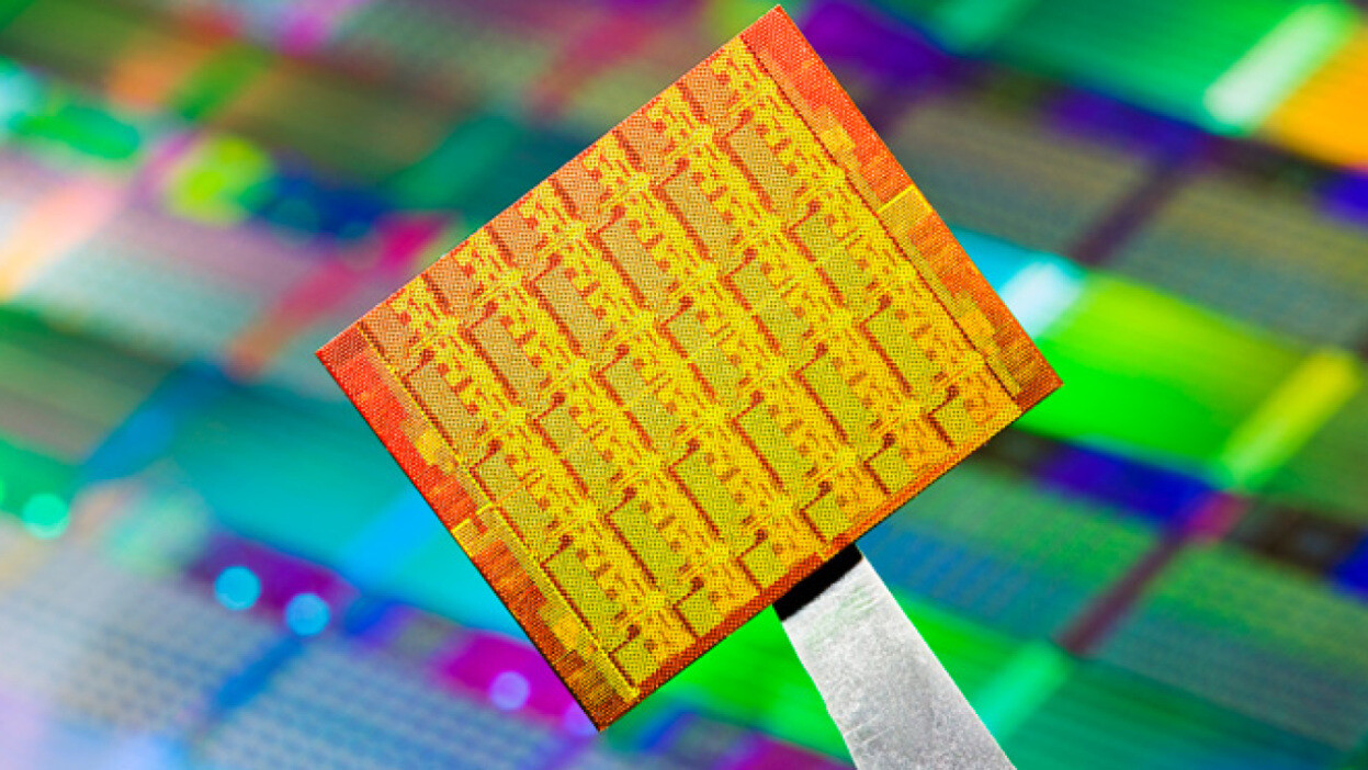
TSMC Unveils Next-Generation HBM4 Base Dies, Built on 12 nm and 5 nm Nodes

During the European Technology Symposium 2024, TSMC has announced its readiness to manufacture next-generation HBM4 base dies using both 12 nm and 5 nm nodes. This significant development is expected to substantially improve the performance, power consumption, and logic density of HBM4 memory, catering to the demands of high-performance computing (HPC) and artificial intelligence (AI) applications. The shift from a traditional 1024-bit interface to an ultra-wide 2048-bit interface is a key aspect of the new HBM4 standard. This change will enable the integration of more logic and higher performance while reducing power consumption. TSMC's N12FFC+ and N5 processes will be used to produce these base dies, with the N12FFC+ process offering a cost-effective solution for achieving HBM4 performance and the N5 process providing even more logic and lower power consumption at HBM4 speeds.

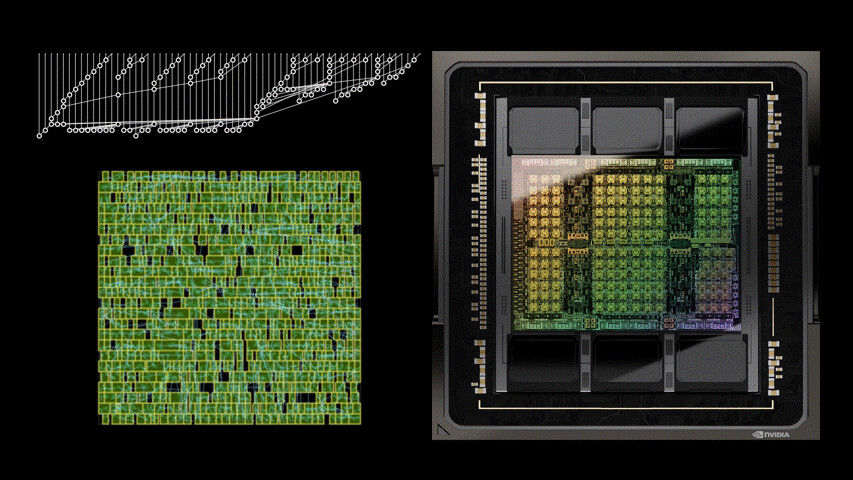
The company is collaborating with major HBM memory partners, including Micron, Samsung, and SK Hynix, to integrate advanced nodes for HBM4 full-stack integration. TSMC's base die, fabricated using the N12FFC+ process, will be used to install HBM4 memory stacks on a silicon interposer alongside system-on-chips (SoCs). This setup will enable the creation of 12-Hi (48 GB) and 16-Hi (64 GB) stacks with per-stack bandwidth exceeding 2 TB/s. TSMC's collaboration with EDA partners like Cadence, Synopsys, and Ansys ensures the integrity of HBM4 channel signals, thermal accuracy, and electromagnetic interference (EMI) in the new HBM4 base dies. TSMC is also optimizing CoWoS-L and CoWoS-R for HBM4 integration, meaning that massive high-performance chips are already utilizing this technology and getting ready for volume manufacturing.

GlobalFoundries and Biden-Harris Administration Announce CHIPS and Science Act Funding for Essential Chip Manufacturing

The U.S. Department of Commerce today announced $1.5 billion in planned direct funding for GlobalFoundries (Nasdaq: GFS) (GF) as part of the U.S. CHIPS and Science Act. This investment will enable GF to expand and create new manufacturing capacity and capabilities to securely produce more essential chips for automotive, IoT, aerospace, defense, and other vital markets.

New York-headquartered GF, celebrating its 15th year of operations, is the only U.S.-based pure play foundry with a global manufacturing footprint including facilities in the U.S., Europe, and Singapore. GF is the first semiconductor pure play foundry to receive a major award (over $1.5 billion) from the CHIPS and Science Act, designed to strengthen American semiconductor manufacturing, supply chains and national security. The proposed funding will support three GF projects:

Synopsys to Acquire Ansys, Creating a Leader in Silicon to Systems Design Solutions

Synopsys (NASDAQ: SNPS) and Ansys (NASDAQ: ANSS) today announced that they have entered into a definitive agreement under which Synopsys will acquire Ansys. Under the terms of the agreement, Ansys shareholders will receive $197.00 in cash and 0.3450 shares of Synopsys common stock for each Ansys share, representing an enterprise value of approximately $35 billion based on the closing price of Synopsys common stock on December 21, 2023. Bringing together Synopsys' pioneering semiconductor electronic design automation (EDA) with Ansys' broad simulation and analysis portfolio will create a leader in silicon to systems design solutions.

"The megatrends of AI, silicon proliferation and software-defined systems are requiring more compute performance and efficiency in the face of growing, systemic complexity. Bringing together Synopsys' industry-leading EDA solutions with Ansys' world-class simulation and analysis capabilities will enable us to deliver a holistic, powerful and seamlessly integrated silicon to systems approach to innovation to help maximize the capabilities of technology R&D teams across a broad range of industries," said Sassine Ghazi, President and CEO of Synopsys. "This is the logical next step for our successful, seven-year partnership with Ansys and I look forward to working closely with Ajei and the talented Ansys team to realize the benefits of this combination for our customers, shareholders and employees."

Synopsys Expands Its ARC Processor IP Portfolio with New RISC-V Family

Synopsys, Inc. (Nasdaq: SNPS) today announced it has extended its ARC Processor IP portfolio to include new RISC-V ARC-V Processor IP, enabling customers to choose from a broad range of flexible, extensible processor options that deliver optimal power-performance efficiency for their target applications. Synopsys leveraged decades of processor IP and software development toolkit experience to develop the new ARC-V Processor IP that is built on the proven microarchitecture of Synopsys' existing ARC Processors, with the added benefit of the expanding RISC-V software ecosystem.

Synopsys ARC-V Processor IP includes high-performance, mid-range, and ultra-low power options, as well as functional safety versions, to address a broad range of application workloads. To accelerate software development, the Synopsys ARC-V Processor IP is supported by the robust and proven Synopsys MetaWare Development Toolkit that generates highly efficient code. In addition, the Synopsys.ai full-stack AI-driven EDA suite is co-optimized with ARC-V Processor IP to provide an out-of-the-box development and verification environment that helps boost productivity and quality-of-results for ARC-V-based SoCs.

Artificial Intelligence Helped Tape Out More than 200 Chips

In its recent Second Quarter of the Fiscal Year 2023 conference, Synopsys issued interesting information about the recent moves of chip developers and their usage of artificial intelligence. As the call notes, over 200+ chips have been taped out using Synopsys DSO.ai place-and-route (PnR) tool, making it a successful commercially proven AI chip design tool. The DSO.ai uses AI to optimize the placement and routing of the chip's transistors so that the layout is compact and efficient with regard to the strict timing constraints of the modern chip. According to Aart J. de Geus, CEO of Synopsys, "By the end of 2022, adoption, including 9 of the top 10 semiconductor vendors have moved forward at great speed with 100 AI-driven commercial tape-outs. Today, the tally is well over 200 and continues to increase at a very fast clip as the industry broadly adopts AI for design from Synopsys."

This is an interesting fact that means that customers are seeing the benefits of AI-assisted tools like DSO.ai. However, the company is not stopping there, and a whole suite of tools is getting an AI makeover. "We unveiled the industry's first full-stack AI-driven EDA suite, sydnopsys.ai," noted the CEO, adding that "Specifically, in parallel to second-generation advances in DSO.ai we announced VSO.ai, which stands for verification space optimization; and TSO.ai, test space optimization. In addition, we are extending AI across the design stack to include analog design and manufacturing." Synopsys' partners in this include NVIDIA, TSMC, MediaTek, Renesas, and IBM Research, all of which used AI-assisted tools for chip design efforts. A much wider range of industry players is expected to adopt these tools as chip design costs continue to soar as we scale the nodes down. With future 3 nm GPU costing an estimated $1.5 billion, 40% of that will account for software, and Synopsys plans to take a cut in that percentage.

NVIDIA GeForce RTX 4060 Ti to Feature a PCI-Express 4.0 x8 Bus Interface

NVIDIA has traditionally refrained from lowering the PCIe lane counts on its mid-range GPUs, doing so only with its most entry-level SKUs, however, this is about to change with the GeForce RTX 40-series. A VideoCardz report says that the upcoming GeForce RTX 4060 Ti, based on the AD106 silicon, comes with a host interface of PCI-Express 4.0 x8.

While this is still plenty of interface bandwidth for a GPU of this market segment, with bandwidth comparable to that of PCI-Express 3.0 x16, using the RTX 4060 Ti on older platforms, such as 10th Gen Intel Core "Comet Lake," or even much newer processors such as the AMD Ryzen 5700G "Cezanne," would run the GPU at PCI-Express 3.0 x8, as the GPU physically lacks the remaining 8 lanes. The lower PCIe lane count should simplify board design for AIC partners, as it reduces the PCB traces and SMDs associated with each individual PCIe lane. Much like DRAM chip traces, PCIe traces are meticulously designed by EDA software (and later validated), to be of equal length across all lanes, for signal integrity.

Huawei Reportedly Develops Chip Design Tools for 14 nm and Above

Amid the US sanctions, Chinese technology giant Huawei has reportedly developed tools to create processors with 14 nm and above lithography. According to Chinese media Yicai, Huawei and its semiconductor partners have teamed up to create replacement tools in place of US chip toolmakers like Cadence, Synopsys, and Mentor/Siemens. These three companies control all of the world's Electronic Design Automation (EDA) tools used for every step of chip design, from architecture to placement and routing to the final physical layout. Many steps need to be taken before making a tapeout of a physical chip, and Huawei's newly developed EDA tools will help the Chinese industry with US sanctions which crippled Huawei for a long time.

Having no access to US-made chipmaking tools, Huawei has invested substantial time into making these EDA tools. However, with competing EDA makers supporting lithography way below 14 nm, Huawei's job still needs to be completed. Chinese semiconductor factories are currently capable of 7 nm chip production, and Huawei itself is working on making a sub-7 nm EUV scanner to aid manufacturing goals and compete with the latest from TSMC and other. If Huawei can create EUV scanners that can achieve transistor sizes smaller than 7 nm, we expect to see their EDA tools keep pace as well. It is only a matter of time before they announce adaptation for smaller nodes.

Open Compute Project Foundation and JEDEC Announce a New Collaboration

Today, the Open Compute Project Foundation (OCP), the nonprofit organization bringing hyperscale innovations to all, and JEDEC Solid State Technology Association, the global leader in the development of standards for the microelectronics industry, announce a new collaboration to establish a framework for the transfer of technology captured in an OCP-approved specification to JEDEC for inclusion in one of its standards. This alliance brings together members from both the OCP and JEDEC communities to share efforts in developing and maintaining global standards needed to advance the electronics industry.

Under this new alliance, the current effort will be to provide a mechanism to standardize Chiplet part descriptions leveraging OCP Chiplet Data Extensible Markup Language (CDXML) specification to become part of JEDEC JEP30: Part Model Guidelines for use with today's EDA tools. With this updated JEDEC standard, expected to be published in 2023, Chiplet builders will be able to provide electronically a standardized Chiplet part description to their customers paving the way for automating System in Package (SiP) design and build using Chiplets. The description will include information needed by SiP builders such as Chiplet thermal properties, physical and mechanical requirements, behavior specifications, power and signal integrity properties, testing the Chiplet in package, and security parameters.

Arm Could Change Licensing Model to Charge OEMs Directly

Over the past few weeks, the legal dispute between Arm Ltd. and Qualcomm Inc. has been warming up the eyes of the entire tech community. However, as per the latest court filing, Arm could change its licensing strategy and shift its whole business model into a new direction that would benefit the company directly. Currently, the company provides the intellectual property (IP) that chip makers can use and add to designs mixed with other IPs and custom in-house solutions. That is how the world of electronics design (EDA) works and how many companies operate. However, in the Qualcomm-Arm legal battle, Qualcomm's counterclaim has brought new light about Arm's plans for licensing its hardware designs past 2024.

According to Dylan Patel of SemiAnalysis, who examined court documents, Arm will reportedly change terms to use its IP where the use of other IP mixed with Arm IP is prohibited. If a chip maker plans to use Arm CPU IP, they must also use Arm's GPU/NPU/ISP/DSP IPs. This would result in devices that utilize every design the UK-based designer has to offer, and other IP makers will have to exclude their designs from the SoC. By doing this, Arm directly stands against deals like the Samsung-AMD deal, where AMD provides RDNA GPU IP and would force Samsung to use Arm's Mali GPU IP instead. This change should take effect in 2025 when every new license agreement has to comply with new rules.

Samsung Electronics Unveils Plans for 1.4 nm Process Technology

Samsung Electronics, a world leader in advanced semiconductor technology, announced today a strengthened business strategy for its Foundry Business with the introduction of cutting-edge technologies at its annual Samsung Foundry Forum event. With significant market growth in high-performance computing (HPC), artificial intelligence (AI), 5/6G connectivity and automotive applications, demand for advanced semiconductors has increased dramatically, making innovation in semiconductor process technology critical to the business success of foundry customers. To that end, Samsung highlighted its commitment to bringing its most advanced process technology, 1.4-nanometer (nm), for mass production in 2027.

During the event, Samsung also outlined steps its Foundry Business is taking in order to meet customers' needs, including: foundry process technology innovation, process technology optimization for each specific applications, stable production capabilities, and customized services for customers. "The technology development goal down to 1.4 nm and foundry platforms specialized for each application, together with stable supply through consistent investment are all part of Samsung's strategies to secure customers' trust and support their success," said Dr. Si-young Choi, president and head of Foundry Business at Samsung Electronics. "Realizing every customer's innovations with our partners has been at the core of our foundry service."

US Institutes GAA-FET Technology EDA Software Ban on China, Stalling sub-3nm Nodes

The US Government has instituted a ban on supply of GAA-FET EDA software to China (the Chinese government and companies in China). Humans can no longer design every single circuit on chips with tens of billions of transistors, and so EDA (electronics design automation) software is used to micromanage design based broadly on what chip architects want. Synopsys, Cadence, and Siemens are major EDA software suppliers. Intel is rumored to use an in-house EDA software that it doesn't sell, although this could change with the company roping in third-party foundries, such as TSMC, for cutting-edge logic chips (which will need the software to make sense of Intel's designs).

GAA or "gates-all-around" technology is vital to building transistors in the 3 nm and 2 nm silicon fabrication nodes. Samsung is already using GAA for its 3 nm node, while TSMC intends to use it with its 2N (2 nm) node. Intel is expected to use it with its Intel 20A (20 angstrom, or 2 nanometers) node. Both Intel and TSMC will debut nodes powered by GAAFETs for mass-production in 2024. The US Government has already banned the sales of EUV lithography machines to China, as well as machines fabricating 3D NAND flash chips with greater than 128 layers or 14 nm. In the past, technology embargoes have totally stopped China from copying or reverse-engineering western tech, or luring Taiwanese engineers armed with industry secrets away on the promise of wealth and a comfortable life in the Mainland.

Microsoft Azure Joins Intel Foundry Services Cloud Alliance

The recent semiconductor shortage has put an unprecedented amount of focus on the industry. Both commercial and government entities have come to recognize the lack of advanced node semiconductor manufacturing capabilities onshore in the United States. Intel Foundry Services (IFS) entry into the commercial foundry space is poised to change all that. As part of IFS Accelerator program, Intel recently announced their new IFS Cloud Alliance program, with Microsoft Azure as one of the inaugural members.

This is the latest chapter in a partnership between Intel and Microsoft that stretches back decades all the way back to the early days of the personal computer. In the last few years, Intel and Microsoft have collaborated on advancing semiconductor design on the cloud by working together to bring out EDA centric cloud compute such as the FX series on Azure, working with EDA vendors to enhance their software to better take advantage of the elasticity of the Azure cloud, as well as collaborating on a secure cloud-based semiconductor development platform for the US Department of Defense RAMP and RAMP-C programs.

NVIDIA PrefixRL Model Designs 25% Smaller Circuits, Making GPUs More Efficient

When designing integrated circuits, engineers aim to produce an efficient design that is easier to manufacture. If they manage to keep the circuit size down, the economics of manufacturing that circuit is also going down. NVIDIA has posted on its technical blog a technique where the company uses an artificial intelligence model called PrefixRL. Using deep reinforcement learning, NVIDIA uses the PrefixRL model to outperform traditional EDA (Electronics Design Automation) tools from major vendors such as Cadence, Synopsys, or Siemens/Mentor. EDA vendors usually implement their in-house AI solution to silicon placement and routing (PnR); however, NVIDIA's PrefixRL solution seems to be doing wonders in the company's workflow.

Creating a deep reinforcement learning model that aims to keep the latency the same as the EDA PnR attempt while achieving a smaller die area is the goal of PrefixRL. According to the technical blog, the latest Hopper H100 GPU architecture uses 13,000 instances of arithmetic circuits that the PrefixRL AI model designed. NVIDIA produced a model that outputs a 25% smaller circuit than comparable EDA output. This is all while achieving similar or better latency. Below, you can compare a 64-bit adder design made by PrefixRL and the same design made by an industry-leading EDA tool.

AMD Selects Google Cloud to Provide Additional Scale for Chip Design Workloads

Google Cloud and AMD today announced a technology partnership in which AMD will run electronic design automation (EDA) for its chip-design workloads on Google Cloud, further extending the on-premises capabilities of AMD data centers. AMD will also leverage Google Cloud's global networking, storage, artificial intelligence, and machine learning capabilities to further improve upon its hybrid and multicloud strategy for these EDA workloads.

Scale, elasticity, and efficient utilization of resources play critical roles in chip design, particularly given that the demand for compute processing grows with each node advancement. To remain flexible and scale easily, AMD will add Google Cloud's newest compute-optimized C2D VM instance, powered by 3rd Gen AMD EPYC processors, to its suite of resources focused on EDA workloads. By leveraging Google Cloud, AMD anticipates being able to run more designs in parallel, giving the team more flexibility to manage short-term compute demands, without reducing allocation on long-term projects.

Google Uses Artificial Intelligence to Develop Faster and Smaller Hardware Accelerators

Designing Artificial Intelligence / Machine Learning hardware accelerators takes effort from hardware engineers in conjunction with scientists working in the AI/ML area itself. A few years ago, we started seeing AI incorporated into parts of electronic design automation (EDA) software tools, helping chip designers speed up the process of creating hardware. What we were "used to" seeing AI do are just a couple of things like placement and routing. And having that automated is a huge deal. However, it looks like the power of AI for chip design is not going to stop there. Researchers at Google and UC Berkeley have made a research project that helps AI design and develop AI-tailored accelerators smaller and faster than anything humans made.

In the published paper, researchers present PRIME - a framework that created AI processors based on a database of blueprints. The PRIME framework feeds off an offline database containing accelerator designs and their corresponding performance metrics (e.g., latency, power, etc.) to design next-generation hardware accelerators. According to Google, PRIME can do so without further hardware simulation and has processors ready for use. As per the paper, PRIME improves performance upon state-of-the-art simulation-driven methods by as much as 1.2x-1.5x. It also reduces the required total simulation time by 93% and 99%, respectively. The framework is also capable of architecting accelerators for unseen applications.

TSMC Expands Advanced Technology Leadership with N4P Process

TSMC today introduced its N4P process, a performance-focused enhancement of the 5-nanometer technology platform. N4P joins the industry's most advanced and extensive portfolio of leading-edge technology processes. With N5, N4, N3 and the latest addition of N4P, TSMC customers will have multiple and compelling choices for power, performance, area, and cost for its products.

As the third major enhancement of TSMC's 5 nm family, N4P will deliver an 11% performance boost over the original N5 technology and a 6% boost over N4. Compared to N5, N4P will also deliver a 22% improvement in power efficiency as well as a 6% improvement in transistor density. In addition, N4P lowers process complexity and improves wafer cycle time by reducing the number of masks. N4P demonstrates TSMC's pursuit and investment in continuous improvement of our process technologies.

AWS and Arm Demonstrate Production-Scale Electronic Design Automation in the Cloud

Today, Amazon Web Services, Inc. (AWS), an Amazon.com, Inc. company, announced that Arm, a global leader in semiconductor design and silicon intellectual property development and licensing, will leverage AWS for its cloud use, including the vast majority of its electronic design automation (EDA) workloads. Arm is migrating EDA workloads to AWS, leveraging AWS Graviton2-based instances (powered by Arm Neoverse cores), and leading the way for transformation of the semiconductor industry, which has traditionally used on-premises data centers for the computationally intensive work of verifying semiconductor designs.

To carry out verification more efficiently, Arm uses the cloud to run simulations of real-world compute scenarios, taking advantage of AWS's virtually unlimited storage and high-performance computing infrastructure to scale the number of simulations it can run in parallel. Since beginning its AWS cloud migration, Arm has realized a 6x improvement in performance time for EDA workflows on AWS. In addition, by running telemetry (the collection and integration of data from remote sources) and analysis on AWS, Arm is generating more powerful engineering, business, and operational insights that help increase workflow efficiency and optimize costs and resources across the company. Arm ultimately plans to reduce its global datacenter footprint by at least 45% and its on-premises compute by 80% as it completes its migration to AWS.

Arm Offers Startups Zero-cost Access to its IP Portfolio

Arm today announced the launch of Arm Flexible Access for Startups, an extension of its already highly successful Flexible Access program. This new initiative offers early-stage silicon startups zero-cost access to a huge range of Arm's leading IP, along with global support and training resources, enabling them to start on their journey to commercial silicon and business scale.

"In today's challenging business landscape, enabling innovation is critical - now more than ever, startups with brilliant ideas need the fastest, most trusted route to success and scale," said Dipti Vachani, senior vice president and general manager, Automotive and IoT Line of Business, Arm. "Arm Flexible Access for Startups offers new silicon entrants a faster, more cost-efficient path to working prototypes, resulting in strengthened investor confidence for future funding."
Arm Chip

DARPA to Dedicate $100 million to EDA Projects Over the Next Five Years

EDA (Electronic Design Automation) is a quintessential part of modern silicon processor design - of any kind. Be it GPUs, CPUs, or SOCs, you can bet an electronic design tool has been applied somewhere in the process. These tools serve their function in various steps of silicon design, be it allowing for automated placement of components, signal routing, power optimization, and analyzing said designs with performance and bottleneck projections. It was rumored that Bulldozer was such a flawed architecture due to the overuse (and misuse) of EDA tools in its design; but mostly, usage of these tools is done in conjunction with engineers' hand-crafted, manually laid-out circuits.

In an effort to accelerate development and reduce cost of chip design (now approaching $500 million for a bleeding-edge SoC), two programs, IDEA (Intelligent Design of Electronic Assets) and POSH (Posh Open Source Hardware), involving 15 companies and more than 200 researchers, will receive $100 million in funding over the next five years. The IDEA is to create the equivalent of a silicon compiler, aimed at significantly lowering the barriers to design chips. POSH aims to create an open-source library of silicon blocks (that circuit designers can then mix and match according to their needs), and IDEA hopes to spawn a variety of open-source and commercial tools to automate testing of those blocks and actually grafting them into SoCs and finished products. Lower development costs means that lower-volume, specialized chips can now be developed more often, thus ushering a new era of specially-designed, fixed-function chips that are more efficient than mass-volume alternatives.
Return to Keyword Browsing
May 20th, 2024 21:06 EDT change timezone

New Forum Posts

Popular Reviews

Controversial News Posts