News Posts matching #Electronic Design Automation

Return to Keyword Browsing

AMD CEO Lisa Su Notes: AI to Dominate Chip Design

Artificial intelligence (AI) has emerged as a transformative force in chip design, with recent examples from China and the United States showcasing its potential. Jensen Huang, CEO of Nvidia, believes that AI can empower individuals to become programmers, while Lisa Su, CEO of AMD, predicts an era where AI dominates chip design. During the 2023 World Artificial Intelligence Conference (WAIC) in Shanghai, Su emphasized the importance of interdisciplinary collaboration for the next generation of chip designers. To excel in this field, engineers must possess a holistic understanding of hardware, software, and algorithms, enabling them to create superior chip designs that meet system usage, customer deployment, and application requirements.

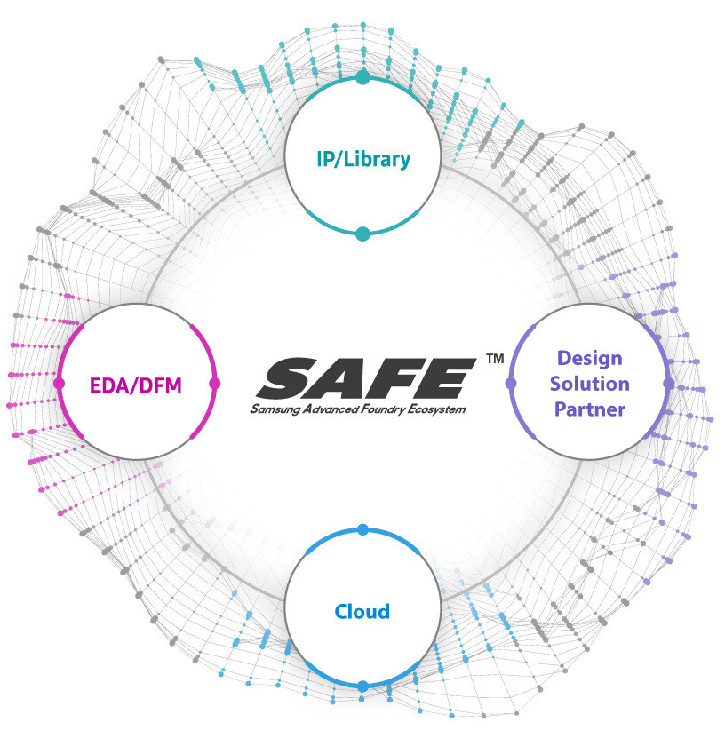
The integration of AI into chip design processes has gained momentum, fueled by the AI revolution catalyzed by large language models (LLMs). Both Huang and Mark Papermaster, CTO of AMD, acknowledge the benefits of AI in accelerating computation and facilitating chip design. AMD has already started leveraging AI in semiconductor design, testing, and verification, with plans to expand its use of generative AI in chip design applications. Companies are now actively exploring the fusion of AI technology with Electronic Design Automation (EDA) tools to streamline complex tasks and minimize manual intervention in chip design. Despite limited data and accuracy challenges, the "EDA+AI" approach holds great promise. For instance, Synopsys has invested significantly in AI tool research and recently launched Synopsys.ai, the industry's first end-to-end AI-driven EDA solution. This comprehensive solution empowers developers to harness AI at every stage of chip development, from system architecture and design to manufacturing, marking a significant leap forward in AI's integration into chip design workflows.

Huawei Reportedly Develops Chip Design Tools for 14 nm and Above

Amid the US sanctions, Chinese technology giant Huawei has reportedly developed tools to create processors with 14 nm and above lithography. According to Chinese media Yicai, Huawei and its semiconductor partners have teamed up to create replacement tools in place of US chip toolmakers like Cadence, Synopsys, and Mentor/Siemens. These three companies control all of the world's Electronic Design Automation (EDA) tools used for every step of chip design, from architecture to placement and routing to the final physical layout. Many steps need to be taken before making a tapeout of a physical chip, and Huawei's newly developed EDA tools will help the Chinese industry with US sanctions which crippled Huawei for a long time.

Having no access to US-made chipmaking tools, Huawei has invested substantial time into making these EDA tools. However, with competing EDA makers supporting lithography way below 14 nm, Huawei's job still needs to be completed. Chinese semiconductor factories are currently capable of 7 nm chip production, and Huawei itself is working on making a sub-7 nm EUV scanner to aid manufacturing goals and compete with the latest from TSMC and other. If Huawei can create EUV scanners that can achieve transistor sizes smaller than 7 nm, we expect to see their EDA tools keep pace as well. It is only a matter of time before they announce adaptation for smaller nodes.

Samsung Electronics Unveils Plans for 1.4 nm Process Technology

Samsung Electronics, a world leader in advanced semiconductor technology, announced today a strengthened business strategy for its Foundry Business with the introduction of cutting-edge technologies at its annual Samsung Foundry Forum event. With significant market growth in high-performance computing (HPC), artificial intelligence (AI), 5/6G connectivity and automotive applications, demand for advanced semiconductors has increased dramatically, making innovation in semiconductor process technology critical to the business success of foundry customers. To that end, Samsung highlighted its commitment to bringing its most advanced process technology, 1.4-nanometer (nm), for mass production in 2027.

During the event, Samsung also outlined steps its Foundry Business is taking in order to meet customers' needs, including: foundry process technology innovation, process technology optimization for each specific applications, stable production capabilities, and customized services for customers. "The technology development goal down to 1.4 nm and foundry platforms specialized for each application, together with stable supply through consistent investment are all part of Samsung's strategies to secure customers' trust and support their success," said Dr. Si-young Choi, president and head of Foundry Business at Samsung Electronics. "Realizing every customer's innovations with our partners has been at the core of our foundry service."

AWS and Arm Demonstrate Production-Scale Electronic Design Automation in the Cloud

Today, Amazon Web Services, Inc. (AWS), an Amazon.com, Inc. company, announced that Arm, a global leader in semiconductor design and silicon intellectual property development and licensing, will leverage AWS for its cloud use, including the vast majority of its electronic design automation (EDA) workloads. Arm is migrating EDA workloads to AWS, leveraging AWS Graviton2-based instances (powered by Arm Neoverse cores), and leading the way for transformation of the semiconductor industry, which has traditionally used on-premises data centers for the computationally intensive work of verifying semiconductor designs.

To carry out verification more efficiently, Arm uses the cloud to run simulations of real-world compute scenarios, taking advantage of AWS's virtually unlimited storage and high-performance computing infrastructure to scale the number of simulations it can run in parallel. Since beginning its AWS cloud migration, Arm has realized a 6x improvement in performance time for EDA workflows on AWS. In addition, by running telemetry (the collection and integration of data from remote sources) and analysis on AWS, Arm is generating more powerful engineering, business, and operational insights that help increase workflow efficiency and optimize costs and resources across the company. Arm ultimately plans to reduce its global datacenter footprint by at least 45% and its on-premises compute by 80% as it completes its migration to AWS.

Samsung Provides One-Stop Foundry Design Environment with the Launch of SAFE Cloud Design Platform

Samsung Electronics Co., Ltd., a world leader in advanced semiconductor technology, today announced the launch of 'Samsung Advanced Foundry Ecosystem (SAFE ) Cloud Design Platform (CDP)' for fabless customers, in collaboration with Rescale, a leader in high performance computing (HPC) applications in the cloud. The key highlight feature of Samsung foundry's first SAFE Cloud Design Platform is that it provides a virtual environment to design chips in the cloud. By accessing this platform through the cloud, customers can immediately start designing at anytime and anywhere.

To maximize customers' design convenience, SAFE CDP supports a very secure design condition that has verified with cloud companies. In addition, customers can utilize various Electronic Design Automation (EDA) tools offered by multiple vendors such as Ansys, Cadence, Mentor, a Siemens business and Synopsys. Gaonchips, one of Samsung Foundry's Design Solution Partners, has already tested the SAFE CDP on its 14 nm automotive project using Cadence's Innovus Implementation System and has successfully reduced its design run-time by 30 percent compared to current on-premise execution.

DARPA to Dedicate $100 million to EDA Projects Over the Next Five Years

EDA (Electronic Design Automation) is a quintessential part of modern silicon processor design - of any kind. Be it GPUs, CPUs, or SOCs, you can bet an electronic design tool has been applied somewhere in the process. These tools serve their function in various steps of silicon design, be it allowing for automated placement of components, signal routing, power optimization, and analyzing said designs with performance and bottleneck projections. It was rumored that Bulldozer was such a flawed architecture due to the overuse (and misuse) of EDA tools in its design; but mostly, usage of these tools is done in conjunction with engineers' hand-crafted, manually laid-out circuits.

In an effort to accelerate development and reduce cost of chip design (now approaching $500 million for a bleeding-edge SoC), two programs, IDEA (Intelligent Design of Electronic Assets) and POSH (Posh Open Source Hardware), involving 15 companies and more than 200 researchers, will receive $100 million in funding over the next five years. The IDEA is to create the equivalent of a silicon compiler, aimed at significantly lowering the barriers to design chips. POSH aims to create an open-source library of silicon blocks (that circuit designers can then mix and match according to their needs), and IDEA hopes to spawn a variety of open-source and commercial tools to automate testing of those blocks and actually grafting them into SoCs and finished products. Lower development costs means that lower-volume, specialized chips can now be developed more often, thus ushering a new era of specially-designed, fixed-function chips that are more efficient than mass-volume alternatives.
Return to Keyword Browsing
Jun 11th, 2024 18:11 EDT change timezone

New Forum Posts

Popular Reviews

Controversial News Posts