News Posts matching #Fermi

Return to Keyword Browsing

NVIDIA Fermi-based GeForce GPU Further Delayed?

NVIDIA's next-generation GeForce GPU based on the Fermi architecture is reportedly further delayed to March 2010, up from its originally expected time-frame of January. NVIDIA on its part maintained that Fermi-based GeForce GPUs will be released sometime in Q1 2010, and with a March launch, that would still stand true.

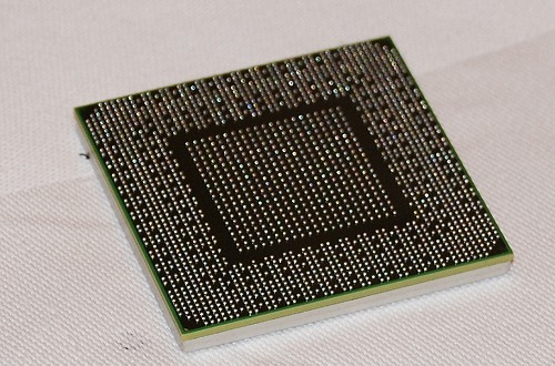
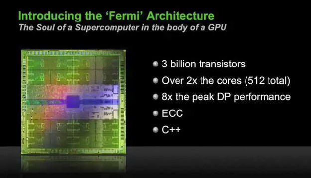
Fermi's development history is marked with late arrivals. The DirectX 11 compliant architecture was announced in October 2009 to counter the market-available DirectX 11 compliant ATI Radeon HD 5800 GPUs. Then in mid-November, the company released the first products based on the architecture - GPGPU accelerators under the NVIDIA Tesla HPC banner. An alleged working prototype GeForce accelerator was spotted around the same time, with word doing rounds that NVIDIA will be ready with the new GeForce GPU in early Q1, probably coinciding with the CES event. Faced with further delays, NVIDIA reportedly notified its partners that the new GPUs will be released to the marked only in March.

NVIDIA plans to launch the 40 nm Fermi-GF100 GPU which is DirectX 11 compliant and supports GDDR5 memory in March, and will launch a GF104 version. Till then, the mainstream-thru-performance segments will be left to be defended by GeForce GTS 250, GT 240, GT 220, 210, 9800 GT, against a fortified mainstream lineup by AMD consisting of ATI Radeon HD 5670/5650 (codenamed "Redwood"), and ATI Radeon HD 5450 (codenamed "Cedar"). These DirectX 11 compliant GPUs from AMD will be released in January.

NVIDIA Pitches GeForce GTX 300 Series to Clinch Performance Crown

NVIDIA's latest DirectX 11 compliant GPU architecture, codenamed "Fermi," is getting its first consumer graphics (desktop) implementation in the form of the GeForce GTX 300 series. The nomenclature turned from being obvious to clear, with a set of company slides being leaked to the media, carrying the GeForce GTX 300 series names for the two products expected to come out first: GeForce GTX 380, and GeForce GTX 360. The three slides in public domain as of now cover three specific game benchmarks, where the two graphics cards are pitted against AMD's Radeon HD 5870 and Radeon HD 5970, being part of the company's internal tests.

Tests include Resident Evil 5 (HQ settings, 1920x1200, 8x AA, DX10), STALKER Clear Sky (Extreme quality, No AA, 1920 x 1200, DX10), and Far Cry 2 (Ultra High Quality, 1920x1200, 8x AA, DX10). Other GPUs include GeForce GTX 295 and GTX 285 for reference, just so you know how NVIDIA is pitting the two against the Radeon HD 5000 GPUs, given that the figures are already out. With all the three tests, GTX 380 emerged on top, with GTX 360 performing close to the HD 5970. A point to note, however, is that the tests were run at 1920 x 1200, and tests have shown that the higher-end HD 5000 series GPUs, particularly the HD 5970, is made for resolutions higher than 1920 x 1200. AA was also disabled in STALKER Clear Sky. NVIDIA's GeForce GTX 300 will be out in Q1 2010.

Update (12/15): NVIDIA's Director of Public Relations EMEAI told us that these slides are fake, but also "when it's ready it's going to be awesome".

NVIDIA Fermi-based GeForce Accelerator Spotted Working

"This puppy here, is Fermi" announced a proud Jen-Hsun Huang, NVIDIA's CEO. The shiny, chrome-decked Tesla GPGPU accelerator that makes use of NVIDIA's Fermi architecture, soon turned out to be a mock-up, aimed solely at announcing the completion of development of the Fermi architecture. It was also strategically timed to coincide with AMD's market launch of the industry's first DirectX 11 compliant graphics cards under the Fermi is significant since it supports the DirectX 11 API. Today ironically, on the occasion of AMD's launch of its "Hemlock" Radeon HD 5970 flagship accelerator, a picture showing a working consumer graphics variant of Fermi working. It is as if to assert that a Fermi derivative is no more the paperweight it was when it was first paraded to the media.

NVIDIA's Fermi GPU architecture is to be implemented in three variants: GF100, GT300, and GT300GL, to drive three of the company's product lines: GeForce, Tesla, and Quadro, respectively. GF100 is of utmost relevance to us. A picture leaked recently to Bright Side of News shows a GeForce accelerator based on GF100 to be working, where it appears to be rendering the Unigine Heaven DirectX 11 benchmark. This early sighting, however, doesn't mean that the product is any closer to its launch. It is still slated for Q1 2010, meaning that it will miss out on the X-Mas shopping season. The GF100 GPU is said to have 512 shader cores, and connects to GDDR5 memory across a 384-bit wide memory interface.

New NVIDIA Tesla GPUs Reduce Cost Of Supercomputing By A Factor Of 10

NVIDIA Corporation today unveiled the Tesla 20-series of parallel processors for the high performance computing (HPC) market, based on its new generation CUDA processor architecture, codenamed "Fermi".

Designed from the ground-up for parallel computing, the NVIDIA Tesla 20-series GPUs slash the cost of computing by delivering the same performance of a traditional CPU-based cluster at one-tenth the cost and one-twentieth the power.

NVIDIA 'Fermi', Tesla Board Pictured in Greater Detail, Non-Functional Dummy Unveiled

Unveiled at the footnote of the GPU Technology Conference 2009, by none other than NVIDIA CEO Jen-Hsun Huang, NVIDIA's Fermi architecture looks promising, at least in the field of GPGPU, which was extensively discussed upon in his address. The first reference board based on NVIDIA's newest 'GT300' GPU is a Tesla HPC processor card, which quickly became the face of the Fermi architecture. Singapore HardwareZone, and PCPop caught some of the first closeup pictures of the Tesla accelerator, and the GPU's BGA itself. Decked in a dash of chrome, the Tesla HPC processor card isn't particularly long, instead a great deal of compacting by its designers is evident. It draws power from one 8-pin, and 6-pin PCI-E power connectors, which aren't located next to each other. The cooler's blower also draws air from openings in the PCB, and a backplate further cools the GPU (and possibly other components located) from behind. From the looks of it, the GPU package itself isn't larger than that of the GT200 or its predecessor, the G80. Looks like NVIDIA is ready with a working prototype against all odds, after all, doesn't it? Not quite. On close inspection of the PCB, it doesn't look like a working sample. Components that are expected to have pins protruding soldered on the other side, don't have them, and the PCB seems to be abruptly ending. Perhaps it's only a dummy made to display at GTC, and give an indication of how the card ends up looking like. In other words, it doesn't look like NVIDIA has a working prototype/sample of the card they intended to have displayed the other day.

NVIDIA Unveils Next Generation CUDA GPU Architecture – Codenamed ''Fermi''

NVIDIA Corp. today introduced its next generation CUDA GPU architecture, codenamed "Fermi". An entirely new ground-up design, the "Fermi" architecture is the foundation for the world's first computational graphics processing units (GPUs), delivering breakthroughs in both graphics and GPU computing.

"NVIDIA and the Fermi team have taken a giant step towards making GPUs attractive for a broader class of programs," said Dave Patterson, director Parallel Computing Research Laboratory, U.C. Berkeley and co-author of Computer Architecture: A Quantitative Approach. "I believe history will record Fermi as a significant milestone."

NVIDIA GT300 ''Fermi'' Detailed

NVIDIA's upcoming flagship graphics processor is going by a lot of codenames. While some call it the GF100, others GT300 (based on the present nomenclature), what is certain that the NVIDIA has given the architecture an internal name of "Fermi", after the Italian physicist Enrico Fermi, the inventor of the nuclear reactor. It doesn't come as a surprise, that the codename of the board itself is going to be called "reactor", according to some sources.

Based on information gathered so far about GT300/Fermi, here's what's packed into it:
  • Transistor count of over 3 billion
  • Built on the 40 nm TSMC process
  • 512 shader processors (which NVIDIA may refer to as "CUDA cores")
  • 32 cores per core cluster
  • 384-bit GDDR5 memory interface
  • 1 MB L1 cache memory, 768 KB L2 unified cache memory
  • Up to 6 GB of total memory, 1.5 GB can be expected for the consumer graphics variant
  • Half Speed IEEE 754 Double Precision floating point
  • Native support for execution of C (CUDA), C++, Fortran, support for DirectCompute 11, DirectX 11, OpenGL 3.1, and OpenCL
Return to Keyword Browsing
Apr 26th, 2024 21:07 EDT change timezone

New Forum Posts

Popular Reviews

Controversial News Posts