News Posts matching #GT300

Return to Keyword Browsing

NVIDIA Fermi-based GeForce Accelerator Spotted Working

"This puppy here, is Fermi" announced a proud Jen-Hsun Huang, NVIDIA's CEO. The shiny, chrome-decked Tesla GPGPU accelerator that makes use of NVIDIA's Fermi architecture, soon turned out to be a mock-up, aimed solely at announcing the completion of development of the Fermi architecture. It was also strategically timed to coincide with AMD's market launch of the industry's first DirectX 11 compliant graphics cards under the Fermi is significant since it supports the DirectX 11 API. Today ironically, on the occasion of AMD's launch of its "Hemlock" Radeon HD 5970 flagship accelerator, a picture showing a working consumer graphics variant of Fermi working. It is as if to assert that a Fermi derivative is no more the paperweight it was when it was first paraded to the media.

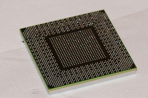
NVIDIA's Fermi GPU architecture is to be implemented in three variants: GF100, GT300, and GT300GL, to drive three of the company's product lines: GeForce, Tesla, and Quadro, respectively. GF100 is of utmost relevance to us. A picture leaked recently to Bright Side of News shows a GeForce accelerator based on GF100 to be working, where it appears to be rendering the Unigine Heaven DirectX 11 benchmark. This early sighting, however, doesn't mean that the product is any closer to its launch. It is still slated for Q1 2010, meaning that it will miss out on the X-Mas shopping season. The GF100 GPU is said to have 512 shader cores, and connects to GDDR5 memory across a 384-bit wide memory interface.

NVIDIA 'Fermi', Tesla Board Pictured in Greater Detail, Non-Functional Dummy Unveiled

Unveiled at the footnote of the GPU Technology Conference 2009, by none other than NVIDIA CEO Jen-Hsun Huang, NVIDIA's Fermi architecture looks promising, at least in the field of GPGPU, which was extensively discussed upon in his address. The first reference board based on NVIDIA's newest 'GT300' GPU is a Tesla HPC processor card, which quickly became the face of the Fermi architecture. Singapore HardwareZone, and PCPop caught some of the first closeup pictures of the Tesla accelerator, and the GPU's BGA itself. Decked in a dash of chrome, the Tesla HPC processor card isn't particularly long, instead a great deal of compacting by its designers is evident. It draws power from one 8-pin, and 6-pin PCI-E power connectors, which aren't located next to each other. The cooler's blower also draws air from openings in the PCB, and a backplate further cools the GPU (and possibly other components located) from behind. From the looks of it, the GPU package itself isn't larger than that of the GT200 or its predecessor, the G80. Looks like NVIDIA is ready with a working prototype against all odds, after all, doesn't it? Not quite. On close inspection of the PCB, it doesn't look like a working sample. Components that are expected to have pins protruding soldered on the other side, don't have them, and the PCB seems to be abruptly ending. Perhaps it's only a dummy made to display at GTC, and give an indication of how the card ends up looking like. In other words, it doesn't look like NVIDIA has a working prototype/sample of the card they intended to have displayed the other day.

NVIDIA GT300 ''Fermi'' Detailed

NVIDIA's upcoming flagship graphics processor is going by a lot of codenames. While some call it the GF100, others GT300 (based on the present nomenclature), what is certain that the NVIDIA has given the architecture an internal name of "Fermi", after the Italian physicist Enrico Fermi, the inventor of the nuclear reactor. It doesn't come as a surprise, that the codename of the board itself is going to be called "reactor", according to some sources.

Based on information gathered so far about GT300/Fermi, here's what's packed into it:
  • Transistor count of over 3 billion
  • Built on the 40 nm TSMC process
  • 512 shader processors (which NVIDIA may refer to as "CUDA cores")
  • 32 cores per core cluster
  • 384-bit GDDR5 memory interface
  • 1 MB L1 cache memory, 768 KB L2 unified cache memory
  • Up to 6 GB of total memory, 1.5 GB can be expected for the consumer graphics variant
  • Half Speed IEEE 754 Double Precision floating point
  • Native support for execution of C (CUDA), C++, Fortran, support for DirectCompute 11, DirectX 11, OpenGL 3.1, and OpenCL

NVIDIA Plans GT300 Demos in September

It looks like NVIDIA doesn't want AMD to drench the media and consumers with enough hype to ensure a smooth, profitable launch of its "Evergreen" family of DirectX 11 GPUs. The party-crasher this time around is NVIDIA's GT300 graphics processor, which sources claim to be continuing on NVIDIA's design methodology of a powerful, monolithic GPU. AMD's itinerary for September looks fairly clear: press-briefings on and around the 10th (we'll be heading to Munich for ours), a number of previews that follow, and launches towards the end of the month, and market availability soon after, in October.

In essence, AMD ends up with all the limelight for the better part of the quarter, in the run up for the crucial November~December shopping season. Meanwhile, the green camp is reportedly readying its own press-briefings of the GT300 GPU. These will be held in late September. To what scale will the briefings be held, or how ready are they with engineering samples is not known as yet, but possibly enough to gain public attention for its DirectX 11 GPUs.

At Least 30% of NVIDIA GPU Shipments on TSMC 40 nm Process by End of 2009

Nearly a month since AMD's introduction of the 40 nm RV740 GPU, there is still no concrete sign of a 40 nm GPU from NVIDIA slated for anytime soon, apart from timely scoops on the GT300. Sources at graphics card vendors however seem confident that by the end of 2009, 40 nm GPUs will constitute at least 30% of NVIDIA's GPU shipments, that too sourced from TSMC, a foundry-partner which has been in the news off late, for technical problems with their 40 nm node, that are affecting its output efficiency.

What's more, NVIDIA seems to have expressed interest in becoming one of the first clients for TSMC's upcoming 28 nm process that is expected to become a reality in Q1 2010. This should also tell you that for GPUs, the next step for silicon fabrication technology will be 28 nm, unlike 32 nm for CPUs.

NVIDIA GT300 Already Taped Out

NVIDIA's upcoming next-generation graphics processor, codenamed GT300 is on course for launch later this year. Its development seems to have crossed an important milestone, with news emerging that the company has already taped out some of the first engineering samples of the GPU, under the A1 batch. The development of the GPU is significant since it is the first high-end GPU to be designed on the 40 nm silicon process. Both NVIDIA and AMD however, are facing issues with the 40 nm manufacturing node of TSMC, the principal foundry-partner for the two. Due to this reason, the chip might be built by another foundry partner (yet to be known) the two are reaching out to. UMC could be a possibility, as it has recently announced its 40 nm node that is ready for "real, high-performance" designs.

The GT300 comes in three basic forms, which perhaps are differentiated by batch quality processing: G300 (that make it to consumer graphics, GeForce series), GT300 (that make it to high-performance computing products, Tesla series), and G200GL (that make it to professional/enterprise graphics, Quadro series). From what we know so far, the core features 512 shader processors, a revamped data processing model in the form of MIMD, and will feature a 512-bit wide GDDR5 memory interface to churn out around 256 GB/s of memory bandwidth. The GPU is compliant with DirectX 11, which makes its entry with Microsoft Windows 7 later this year, and can be found in release candidate versions of the OS already.

GT300 to Boast Around 256 GB/s Memory Bandwidth

Recently, early-information on NVIDIA's next-generation GT300 graphics processor surfaced, that suggested it to pack 512 shader processors, and an enhanced processing model. A fresh report from Hardware-Infos sheds some light on its memory interface, revealing it to be stronger than that of any production GPU. According to a piece of information that has been doing ping-pong between Hardware-Infos and Bright Side of News, GT300 might feature a 512-bit wide GDDR5 memory interface.

The memory interface in conjunction with the use of the lowest latency GDDR5 memory available, at a theoretical 1000 MHz (2000 MHz DDR) would churn out 256 GB/s of bandwidth, the highest for a GPU so far. Although Hardware-Infos puts the lowest-latency figure at 0.5 ns, the math wouldn't work out. At 0.5 ns, memory with actual clock rate of 1000 MHz would churn out 512 GB/s, so a slight inaccuracy there. Qimonda's IDGV1G-05A1F1C-40X leads production today with its "40X" rating. With these chips across a 512-bit interface, the 256 GB/s bandwidth equation is satisfied. The clock speeds of the memory isn't known just as yet, the above is just an example that uses the commonly available high-performance GDDR5 memory chip. The new GPU, at least from these little information leaks, is shaping up to be another silicon-monstrosity by NVIDIA in the making.

GT300 to Pack 512 Shader Processors

A real monster seems to be taking shape at NVIDIA. The company's next big graphics processor looks like a leap ahead of anything current-generation, the way G80 was when it released. It is already learned that the GPU will use a new MIMD (multiple instructions multiple data) mechanism for its highly parallel computing, which will be physically handled by not 384, but 512 shader processors. The count is a 112.5% increase over that of the existing GT200, which has 240.

NVIDIA has reportedly upped the SP count per cluster to 32, against 24 for the current architecture, and a cluster count of 16 (16 x 32 = 512). Also in place, will be 8 texture memory units (TMUs) per cluster, so 128 in all. What exactly makes the GT300 a leap is not only the fact that there is a serious increase in parallelism, but also an elementary change in the way a shader processor handles data and instructions, in theory, a more efficient way of doing it with MIMD. The new GPU will be DirectX 11 compliant, and be built on the 40 nm manufacturing process. We are yet to learn more about its memory subsystem. The GPU is expected to be released in Q4 2009.

ATI Months Ahead of NVIDIA with DirectX 11 GPU Schedule?

Never in recent times have we seen NVIDIA and ATI locked in such fierce market competition. The two are seen exchanging blows with product launches and price-cuts. ATI looks to be in the mood to take this competition to the next-level: DirectX 11 compliant GPUs. Microsoft has already released DirectX 11 with the pre-release versions of Windows 7 operating system. A recent report by Heise Online indicates that AMD will be ready with an ATI RV870, the company's first DirectX 11 GPU by the end of July, or early August.

Another source, The Inquirer, states NVIDIA's GT300 GPU launch for October. If you were to count these claims, AMD is put two to three months ahead of NVIDIA when it comes to time-to-market introduction of a new GPU generation. Now, whether you have DirectX 11 compliant software that makes use of the new technology available that soon is a different thing altogether. This will determine the practicality of a DirectX 11 GPU in July/August.

GT300 A Leap Forward for NVIDIA GPU Architecture

Every once in a while, comes a GPU by NVIDIA that marks the evolution of GPU architecture for NVIDIA. A good example of this would be the G80, which was a distinct evolution of the GPU architecture for the company. Sources tell Hardware-Infos that the GT300 is on course of being one such GPU that comes with distinct architectural changes. To begin with, GT300 will start the company's DirectX 11 conquest the way its ancestor, the G80 did for DirectX 10, which turned out to be largely a successful one.

The GT300's architecture will be based on a new form of number-crunching machinery. While today's NVIDIA GPUs feature a SIMD (single instruction multiple data) computation mechanism, the GT300 will introduce the GPU to MIMD (multiple instructions multiple data) mechanism. This is expected to boost the computational efficiency of the GPU many-fold. The ALU cluster organization will be dynamic, pooled, and driven by a crossbar switch. Once again, NVIDIA gets to drop clock-speeds and power consumptions, while achieving greater levels of performance than current-generation GPUs. With GT300, NVIDIA will introduce the next major update to CUDA. With the new GPUs being built on the 40nm silicon fabrication process, transistor counts are expected to spiral-up. NVIDIA's GT300 is expected to go to office in Q4 2009, with its launch schedule more or less dependent on that of Microsoft's Windows 7 operating system that brings in DirectX 11 support.

NVIDIA GPU Lineup for 2009 Tabled

The year 2008 has been eventful for the PC graphics industry. This is the year which, for the most of the part, saw some serious competition between NVIDIA and ATI. While pure horsepower and value are what determined product superiority, implementing new technologies is what looks to drive GPU makers in 2009. One of the first of these technologies is the introduction of the 40nm manufacturing process, which facilitates GPU makers to step-up transistor counts or even cut manufacturing costs. VR-Zone, based on a few documents it has access to, compiled a list of GPUs that NVIDIA could pull out of its hat in 2009.

To begin with, NVIDIA is expected to have a full-fledged lineup of GPUs top-to-bottom built on the 40nm fab process within 2009. Before it makes the move to the new fab process, the G200b, built on the 55nm fab process will be given a chance to hold the performance and enthusiast segment offerings by the company, in Q1. Come Q2, and the G200b will be succeeded by GT212. All that while, current G94, G96, G98 will hold the mainstream thru value segments, only to be replaced by GT214, GT216 and GT218 respectively in Q3. NVIDIA's gets a newer IGP too, the iGT209. NVIDIA looks to end the year with a newer high-end GPU, the GT300 to succeed GT212 in Q4.

RV740 Successfully Taped Out, Other 40nm GPUs Follow

The RV740 graphics processor by AMD could well be the first GPU in production, to be built on the newer 40nm manufacturing process, giving its makers something to brag about. The RV740 design and specifications are largely derived from the RV770LE (covered here), while bringing the GDDR5 memory standard to the mainstream.

Chinese industrial journals tell DigiTimes that the company has completed taping-out the RV740, and that the GPU is awaiting mass-production by AMD's foundry partner, Taiwan Semiconductor Manufacturing Company (TSMC). Mass production of products based on this GPU could commence by the end of Q1 2009.

NVIDIA to Launch GT300 in Q1 2009?

The tentative release time-frames for upcoming GPUs by NVIDIA and AMD have been seesawing between early 2009 and Q4 2009 for some time now. Industrial sources tell DigiTimes, that NVIDIA will be launching the GT300 graphics processor as early as in Q1 2009. What's even more surprising according to the report, is that the new GPU will be built on the 55nm manufacturing node of its foundry partners.

In related news, NVIDIA will be showcasing its range of products based on the 55nm G200b core at CES 2009, which starts on January 8. The notable products include a dual-GPU card, the GeForce GTX 295, and the single GPU flagship product, the GeForce GTX 285. NVIDIA refused to comment on the report.

Power and Innovation to Drive High-End GPUs in 2009

The year 2008 so far, has been very eventful for the graphics card market. A reinvigorated GPU lineup by ATI, brought in some fierce competition to NVIDIA, which resulted in a tug-of-war with pricing graphics cards in the market, with either company refusing to lose on grounds of pricing. This event, coupled with the announcement of several game titles by game publishers, resulted in bumper-sales of graphics cards, giving the present state of the global economy little or no relevance.

The months to come hold the same amount of importance for both AMD and NVIDIA, where the next round of competition begins with successors to current high-end products being slated. NVIDIA is expected to continue with its monolithic high transistor-count GPU design methodology, while AMD could bring in a little change to the way it uses two efficient GPUs to build powerful products.

40nm High-End NVIDIA GPUs Slated for 2009, GT206 for Q4

NVIDIA is expected to continue on its monolithic high-end GPU approach with a few notable GPUs that have been slated for Q4, 2008 and throughout 2009. The visual computing giant will be rolling out a 55nm derivative of the existing G200 graphics processor, codenamed GT206. The GPU is expected to be essentially the same, albeit newer silicon process allowing higher clock-speeds, that push up the performance envelope. The GT206 will be released in Q4, 2008., presumably to cash-in on the X-mas shopping season. It is found that GT206 seems to be having problems with its shader domain, which has pushed its launch for that late.

Following GT206, GT212 and GT216 would be NVIDIA's entries to the 40nm silicon fabrication process. Earlier reports suggested that foundry companies in Taiwan could be ready with the infrastructure to manufacture 40nm GPUs by June/July 2009. For the late second quarter 2009, either GT212, GT216, or simply a new card based the GT206, in a dual-GPU configuration could lead the pack. GT212 and GT216 could release in Q2, 2009. The GT212, GT216 GPUs support GDDR5 memory on a broad memory bus. Towards the end of the year however, NVIDIA will have made its DirectX 11 GPU, the GT300.

NVIDIA Preparing GT300 Graphics Processor?

Hardspell reports that NVIDIA may have cancelled working on the G200b (the 55nm version of GT200). Details on this new DirectX 10.1 graphics processor trickled in, it has 384 shader units, uses a 45nm fabrication process and incorporates 1 GB of GDDR5 memory at 4.00 GHz (effective) while the core could be clocked at 800 MHz with a 2.00 GHz shader domain. NVIDIA hopes to take on the R700 and its successor which unreliable sources claim to be based on the Super-RV770.
Return to Keyword Browsing
Apr 26th, 2024 08:44 EDT change timezone

New Forum Posts

Popular Reviews

Controversial News Posts