News Posts matching #GV100

Return to Keyword Browsing

EK Water Blocks Unveils EK-FC GV100 Pro, A Water Block for Professionals

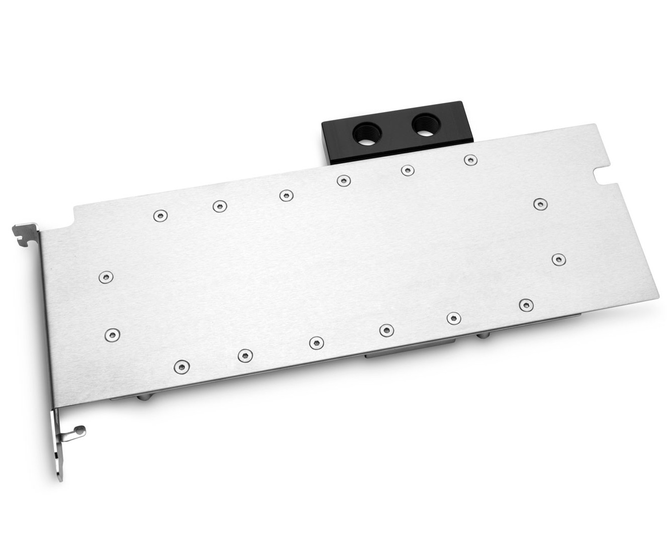
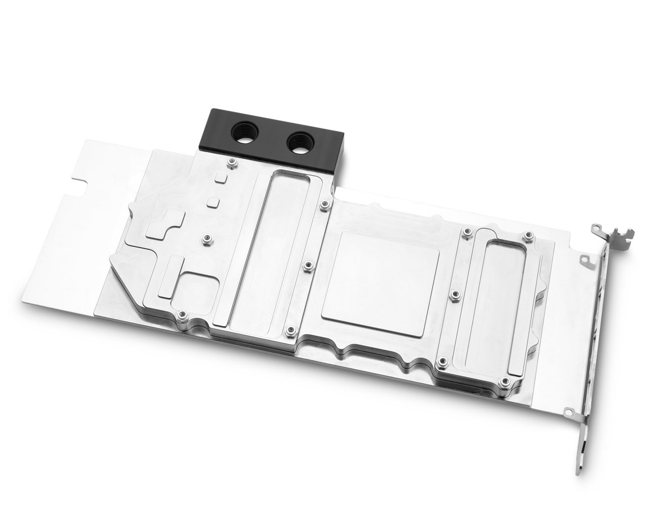
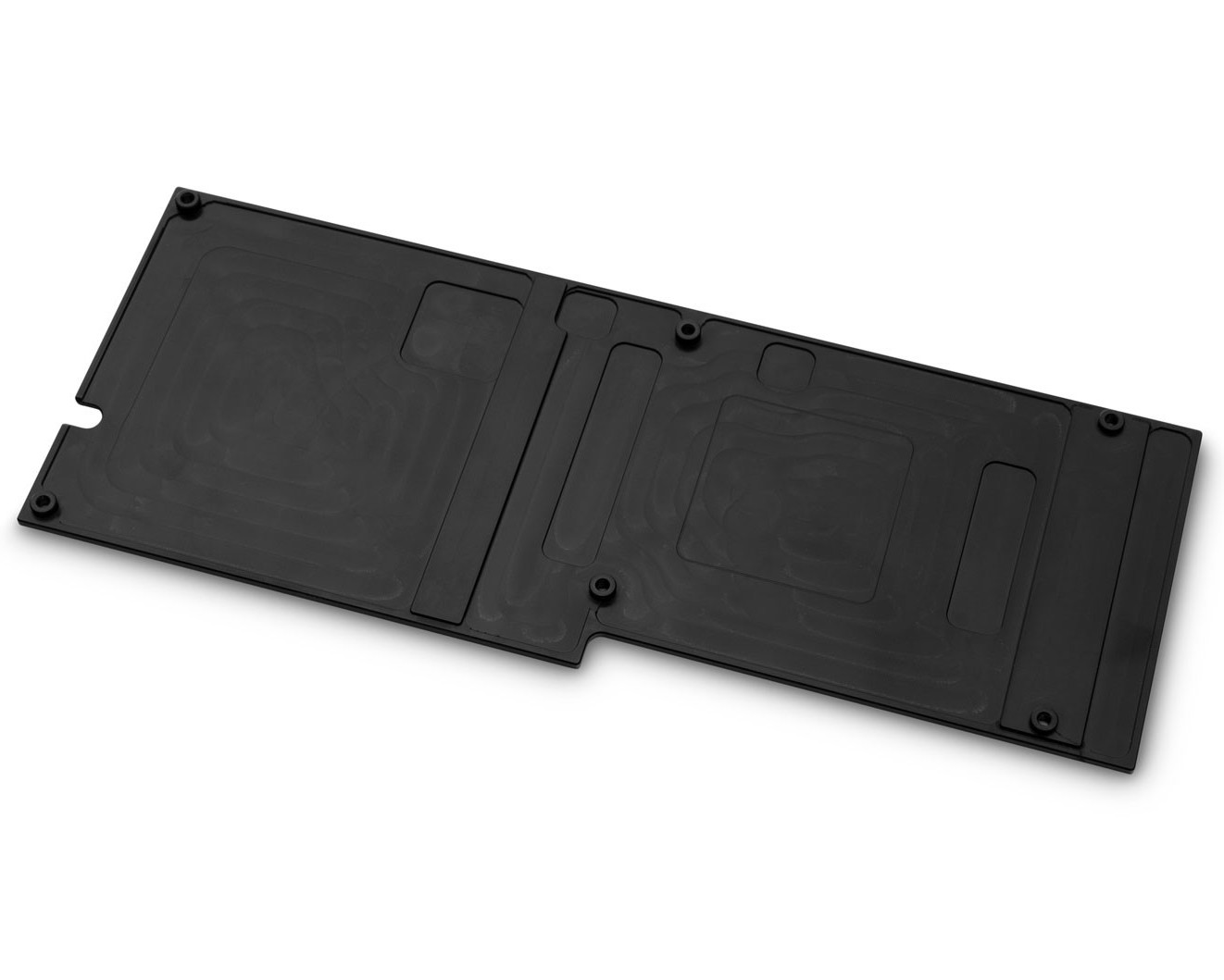
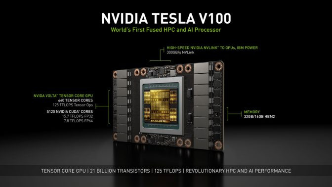
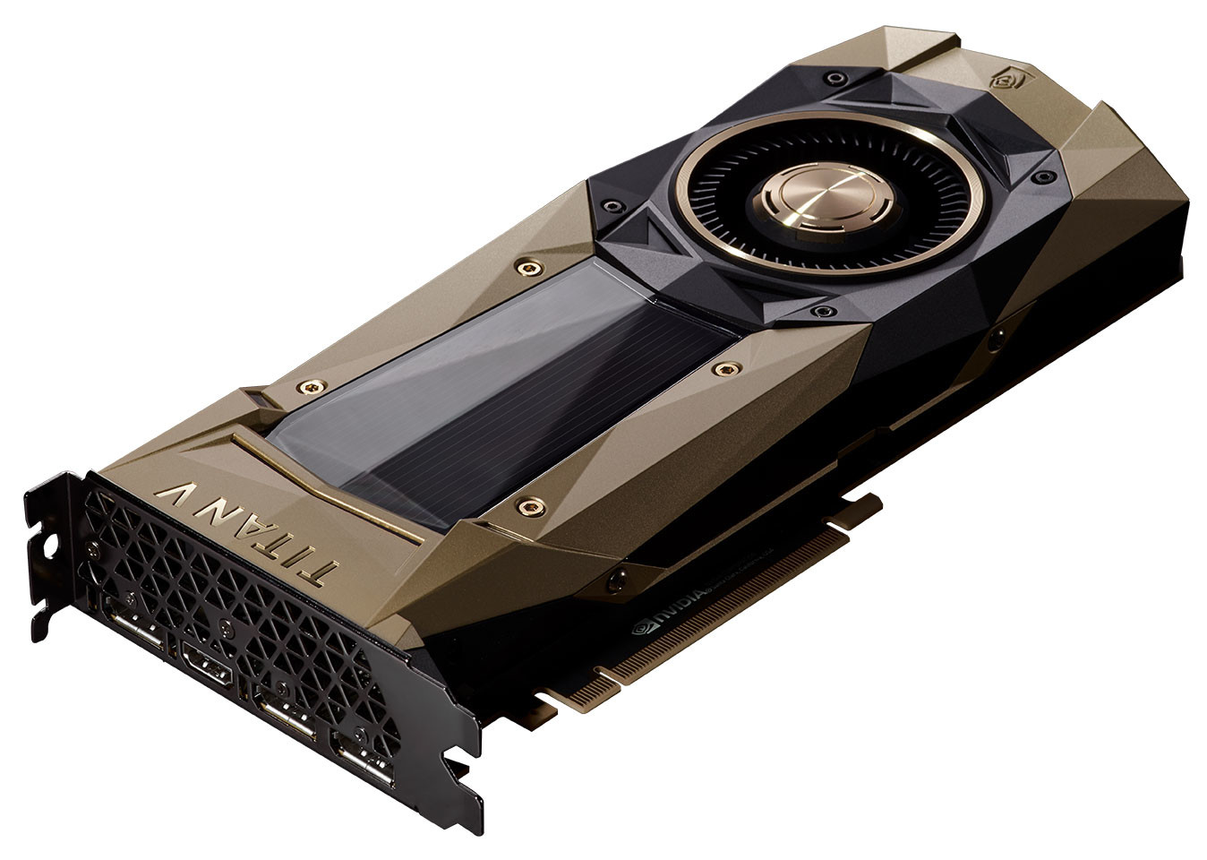
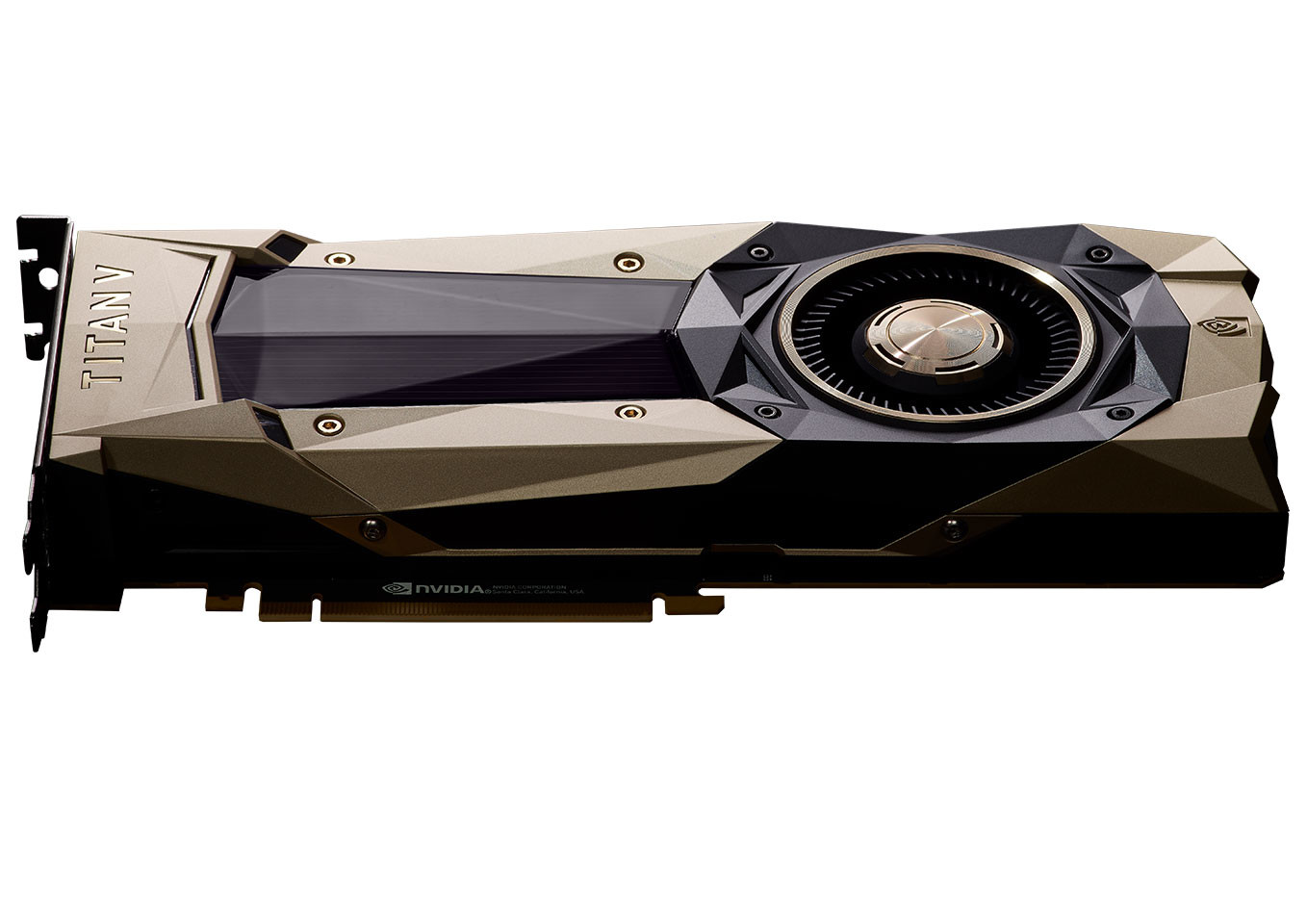
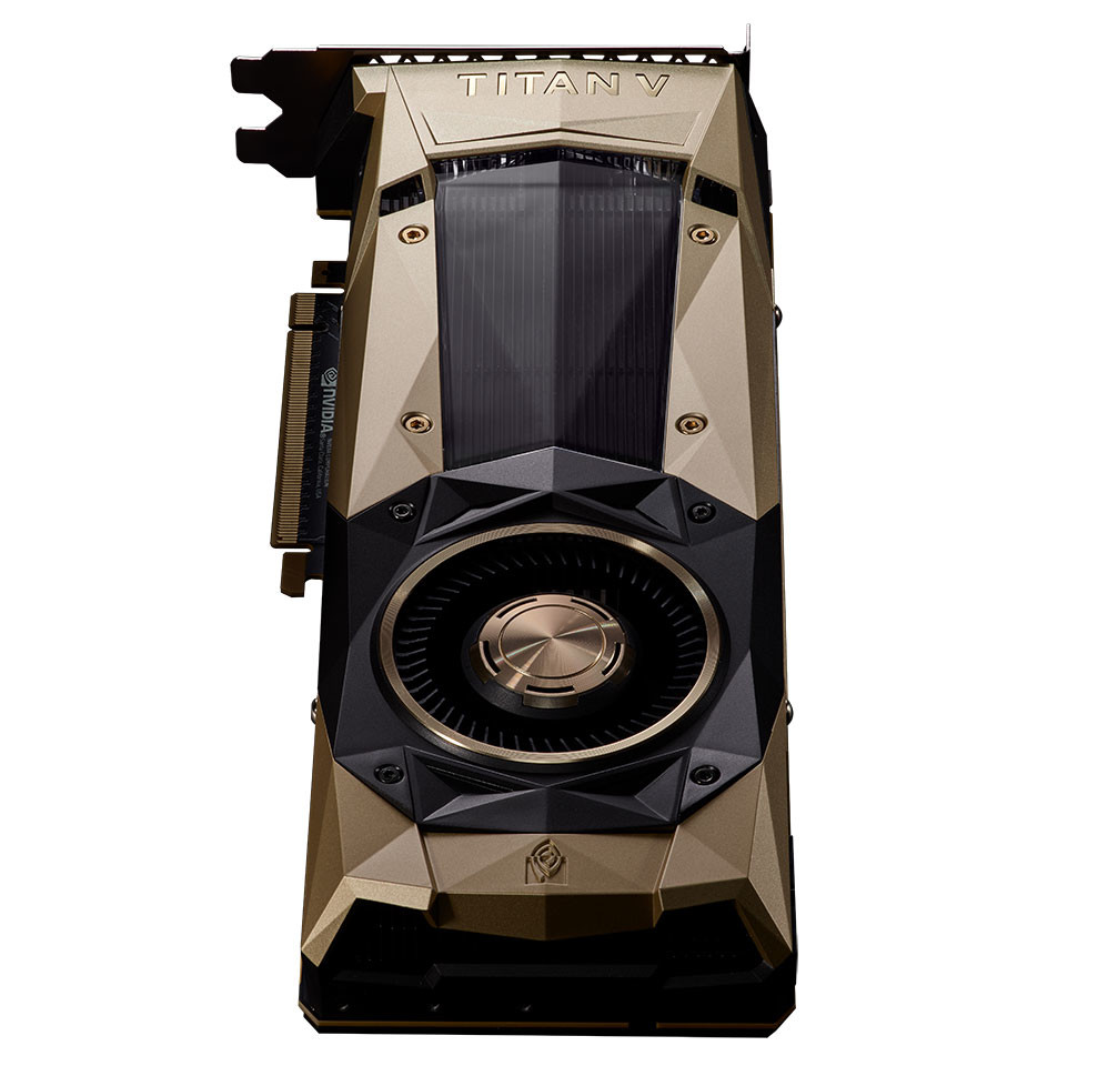
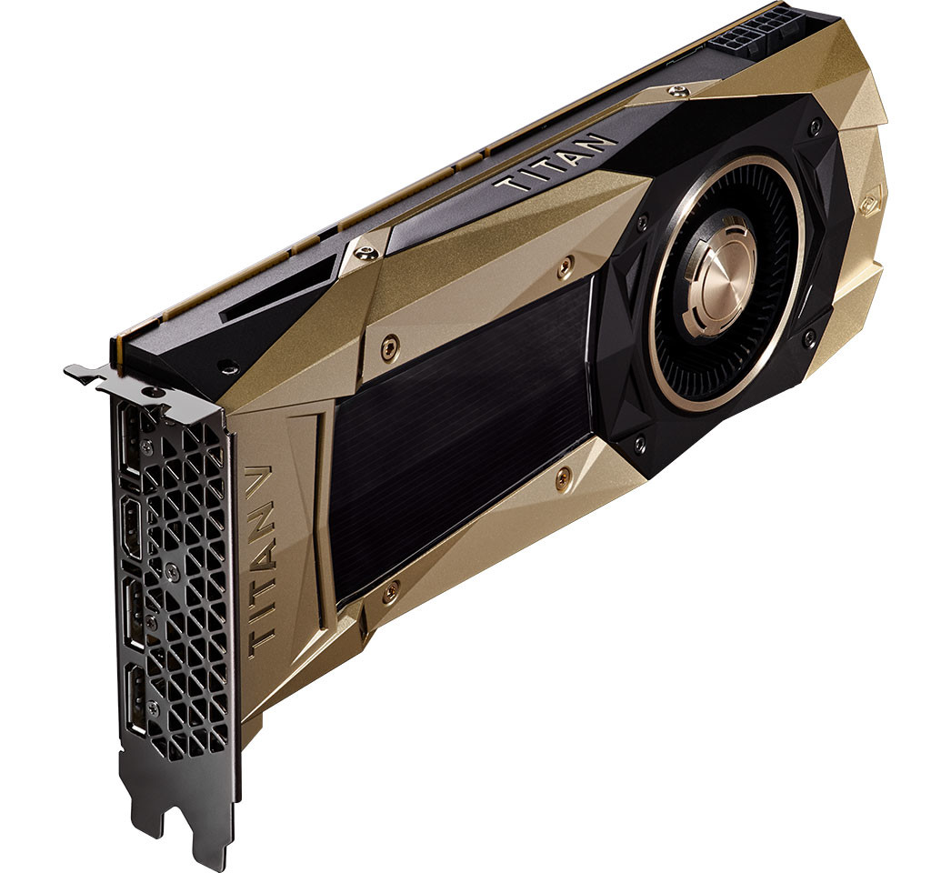
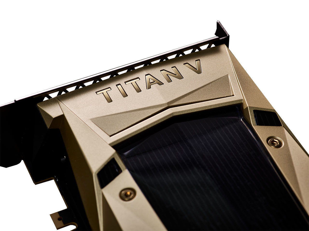
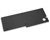
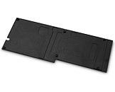
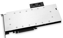
EK Water Blocks, the premium computer liquid cooling gear manufacturer, is releasing a workstation/server grade water block for some of the most powerful Workstation GPUs on the market today based on the NVIDIA GV100 graphic chip. That includes both the Quadro GV100 and Tesla V100, as well as the Titan V. The EK-FC GV100 Pro water block spans across the entire length of the card cooling all critical components.

With the launch of this water block, its clear that EKs plan of expansion into the professional workstation and server grade market is well under way. In the following months you can expect many more worksation and enterprise cooling solutions from EK.

Latest AIDA 64 Beta Adds Support for GV104, GV104M - Mentions GeForce GTX 1180

It seems that speculation on NVIDIA's next-gen naming scheme is coming to a close - finally. FinalWire have recently posted an updated, beta version of their popular AIDA 64 tool, which on its 5.97.4679 beta version comes with a mention for NVIDIA's GV102, GV102GL, GV104 and GV104M silicon. Digging deeper, associated to the GV104 chip, is the Device ID 1e87 - which results in a listing identified as a GeForce GTX 1180. It's not final a reveal yet, but this is a strong indication as to how exactly NVIDIA's naming scheme will pan out.

With Summit, US Regains Leadership from China in TOP500 Supercomputers Listing

We previously covered in more depth the fact that the US was gearing up to overtake China's Sunway TaihuLight, then the world's fastest supercomputer, with its Summit machine, built in collaboration between IBM (with its water-cooled Power Systems AC922 nodes with 24-core processors and 96 processing threads) and NVIDIA (GV100 GPUs).

Now, this US dream has finally come to pass, and in a big way - the Summit delivers more than double the performance of China's posterchild, coming in at 200 PetaFLOPs of computing power. Summit boasts of 27,648 Volta Tensor Core GPUs and 9,216 CPUs within its 5,600 square feet. The Summit supercomputer consumes 15 MW of power (the site where it's deployed is able to deliver up to 20 MW), which is on-par with China's Sunway - but remember, it more than doubles the peak PetaFlops from 93 to 200. A good step in the battle for supercomputer supremacy, but China still has an increasing foothold in the number of systems it has employed and registered with the TOP500.

NVIDIA Quadro GV100 Surfaces in Latest NVFlash Binary

NVIDIA could be giving final touches to its Quadro GV100 "Volta" professional graphics card, after the surprise late-2017 launch of the NVIDIA TITAN V. The card was found listed in the binary view of the latest version of NVFlash (v5.427.0), the most popular NVIDIA graphics card BIOS extraction and flashing utility. Since its feature-set upgrade to the TITAN Xp through newer drivers, NVIDIA has given the TITAN family of graphics cards a quasi-professional differentiation from its GeForce GTX family.

The Quadro family still has the most professional features, software certifications, and are sought after by big companies into graphics design, media, animation, architecture, resource exploration, etc. The Quadro GV100 could hence yet be more feature-rich than the TITAN V. With its GV100 silicon, NVIDIA is using a common ASIC and board design for its Tesla V100 PCIe add-in card variants, the TITAN V, and the Quadro GV100. While the company endowed the TITAN V with 12 GB of HBM2 memory using 3 out of 4 memory stacks the ASIC is capable of holding; there's an opportunity for NVIDIA to differentiate the Quadro GV100 by giving it that 4th memory stack, and 16 GB of total memory. You can download the latest version of NVFlash here.

NVIDIA Announces TITAN V "Volta" Graphics Card

NVIDIA in a shock move, announced its new flagship graphics card, the TITAN V. This card implements the "Volta" GV100 graphics processor, the same one which drives the company's Tesla V100 HPC accelerator. The GV100 is a multi-chip module, with the GPU die and three HBM2 memory stacks sharing a package. The card features 12 GB of HBM2 memory across a 3072-bit wide memory interface. The GPU die has been built on the 12 nm FinFET+ process by TSMC. NVIDIA TITAN V maxes out the GV100 silicon, if not its memory interface, featuring a whopping 5,120 CUDA cores, 640 Tensor cores (specialized units that accelerate neural-net building/training). The CUDA cores are spread across 80 streaming multiprocessors (64 CUDA cores per SM), spread across 6 graphics processing clusters (GPCs). The TMU count is 320.

The GPU core is clocked at 1200 MHz, with a GPU Boost frequency of 1455 MHz, and an HBM2 memory clock of 850 MHz, translating into 652.8 GB/s memory bandwidth (1.70 Gbps stacks). The card draws power from a combination of 6-pin and 8-pin PCIe power connectors. Display outputs include three DP and one HDMI connectors. With a wallet-scorching price of USD $2,999, and available exclusively through NVIDIA store, the TITAN V is evidence that with Intel deciding to sell client-segment processors for $2,000, it was a matter of time before GPU makers seek out that price-band. At $3k, the GV100's margins are probably more than made up for.
Return to Keyword Browsing
Jun 5th, 2024 19:17 EDT change timezone

New Forum Posts

Popular Reviews

Controversial News Posts