News Posts matching #Kepler

Return to Keyword Browsing

Christmas Special: The PC Technology of 2011

Welcome to the TechPowerUp 2011 PC technology Christmas special. We hope that you will enjoy reading it while tucking into your turkey, Christmas presents and a little too much wine... In this article, we go through the technology of 2011 that has had the most significance, the most impact and was generally the most talked about. It's not necessarily the best tech of 2011 which is the most significant though, since lemons can be just as significant as the ground-breakers in how they fail to deliver - and the backlash that goes with it.

January: Intel Sandy Bridge i5 & i7

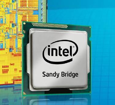
Released on January 9th, the new Intel Core i5 & i7 processors were based on Intel's second generation Core architecture built on a 32 nm production process (HEXUS review). They included an IGP (Integrated Graphics Processor) physically on the same piece of silicon along with HyperThreading. These new dual and quad core processors soundly beat all previous generations of Intel processors in terms of processing performance, heat, power use, features and left AMD in the dust. Therefore, Intel badly needed some competition from AMD and unless you have been living under a rock, you will know how that turned out in October with the launch of Bulldozer. Sandy Bridge was a sound win and is generally considered to be the only architecture worth considering at this point. The i5-2500K is currently at the sweet spot of price/performance. It comes at a stock speed of 3.3 GHz, but typically overclocks to an amazing 4.5 - 5 GHz with a decent air cooler and without too much difficulty in getting there. Models in the budget i3 range were released at various times later. See this Wikipedia article for details.
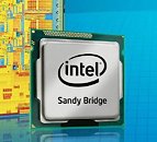
Cost-Effective Radeon HD 7900 PCB Already In The Works

A little earlier today, we showed you pictures of AMD's first Radeon HD 7900 series single-GPU PCB that makes use of digital-PWM power delivery. Some of the first batches of Radeon HD 7900 graphics cards will stick to that PCB and board design, as it's backed by AMD's engineering. Even as the SKU's launch is less than 24 hours away, there are pictures of AMD's cost-effective Radeon HD 7900 PCB surfacing on Asian media sites. Once ready, AMD add-in board partners can opt for this cost-effective PCB if they want to fine-tune their prices. It looks like AMD is ready well ahead to face competition from NVIDIA, with its GeForce Kepler 104 (GK104) GPU.

The cost-effective PCB, without any components laid, is pictured below. The first picture shows its obverse side, the second, its reverse side. The PCB is completely up to speed with everything Tahiti GPU will need. It has provision for two 8-pin PCIe power inputs, an 8+2 phase cost-effective analog VRM, probably driven by a cost-effective CHIL controller, and a different display output connector loadout. It has provision for two DVI, and one each of HDMI and full-size DisplayPort. Partners can still use a single DVI connector, and keep their cards single-slot capable. Provisions for 12 GDDR5 chips are right where they should be. There is nothing eventful in the reverse side, just traces for all the supportive components.

NVIDIA Kepler To Do Away with Hotclocks

Since the days of NVIDIA's very first DirectX 10 GPUs, NVIDIA has been using different clock domains for the shaders and the rest of the GPU (geometry domain). Over the past few generations, the shader clock has been set 2x the geometry domain (the rest of the GPU). 3DCenter.org has learned that with the next-generation "Kepler" family of GPUs, NVIDIA will do away with this "Hotclock" principle. The heavy number-crunching parts of the GPU, the CUDA cores, will run at the same clock-speed as the rest of the GPU.

It is also learned that NVIDIA will have higher core speeds overall. The clock speed of the GK104, for example, is expected to be set "well above 1 GHz", yielding compute power "clearly over 2 TFLOPs" (3DCenter's words). It looks like NVIDIA too will have some significant architectural changes up its sleeve with Kepler.

GeForce Kepler 104 and 100 GPU Specifications Compiled

A quick stroll through our previous article about how the GeForce Kepler family of next-generation GPUs is laid out, would tell you that GeForce Kepler 104 (GK104), is going to be NVIDIA's answer to AMD's Tahiti. GK104 will be a high-performance (≠ high-end) GPU by NVIDIA that will have many of the features that were reserved for its previous high-end GPUs (such as a 384-bit wide GDDR5 memory interface), but will not be NVIDIA's most powerful GPU in the series. The throne will be kept empty for GK100, which will comply with NVIDIA's "go all in" design ideology for high-end GPUs.

3DCenter.org compiled a few specifications of the GK104 and GK100. They go like this:
GK104
  • 640 to 768 CUDA cores
  • 80 to 96 TMUs (depending on what the CUDA core count ends up being)
  • 384-bit GDDR5 memory interface, 48 ROPs
  • Built on the 28 nm TSMC process
  • Products based on this will launch in the first quarter of 2012

NVIDIA GeForce Kepler Roadmap Compiled

2012-13 promises to be a period of big graphics product launches, centric to a new DirectX version, DirectX 11.1, which will ship with Microsoft's next major Windows version (currently referred to as Windows 8). Information compiled by ExpertsPC.com and 4Gamer.net tables what NVIDIA's next-generation graphics family could look like, and around what time it could be released to market. With its next-generation GeForce Kepler family of GPUs, NVIDIA will follow a sensible bottom-up product release model, to ensure that it isn't met with any technical hurdles with TSMC's new 28 nm manufacturing process, and so it could launch GPUs with increasingly higher transistor counts, till its top-of-the-line GPU is outed.

The first GPU in NVIDIA's pipeline is the GeForce Kepler 107 (GK107), on which will be based entry thru lower-mainstream SKUs. The data doesn't reveal things like core counts, but points out that GK107 will have a 128-bit wide GDDR5 memory interface, will use the current-generation PCI-Express 2.0 bus, will be built on the 28 nm process, and will support DirectX 11.1. This will be followed by the GK106, on which "sweet-spot" SKUs could be based. This will be NVIDIA's first PCI-Express 3.0 compliant GPU, it will have a 256-bit wide GDDR5 memory interface.

Are Improving Integrated Graphics Slowly Killing Off Discrete Graphics Cards?

Intel started the trend of improving integrated graphics with their second generation LGA1155 socket Core i3, i5 & i7 line of processors. Depending on the model, these processors sport integrated HD2000 or HD3000 graphics right on the processor die, which nowadays give acceptable performance for low-end gaming and can play Full HD 1080p video perfectly. This trend is increasing with the upcoming Ivy Bridge processors, which will be able to support a massive 4096 x 4096 pixel display, as we reported here. AMD now also have equivalent products with their Llano-based A-series processors. So, where does this leave discrete graphics cards? Well, the low end market is certainly seeing reduced sales, as there really isn't enough of a performance difference nowadays to always warrant an upgrade from an IGP. As integrated graphics improve further, one can see how this will hurt sales of higher end graphics cards too. The problem is that the bulk of the profit comes not from the top-end powerhouse graphics cards, but from the low to mid-end cards which allow these companies to remain in business, so cannibalizing sales of these products to integrated graphics could make high-end graphics cards a much more niche product and crucially, much more expensive with to boot.

Spire Announces Kepler Series Universal CPU Coolers

The Spire all new Kepler universal micro-processor cooler series are direct contact heat-pipe solutions for Core i3/i5 and i7 from Intel and the AMD AM2/3/FM1 micro-processors. There are three (3) different models ranging from two up to four 6mm sinter powder heat-pipes which are in direct contact with the cpu heat-source, dissipating heat effectively and fast.

The high density fins are crowned with a powerful fan for high airflow and great cooling performance. The 92mm dc fan provides ample airflow and silent cooling at 19.0dBA. Compatibility is ensured with the multi-platform mounting clip for Intel 775/1155/1156 sockets and AM2/AM3/FM1 micro-processors. The Kepler series from Spire are build to deliver great cooling for maximum system performance.

GeForce BETA Driver Hints At First GeForce 600 Series Models

If not mission-critical stability, GeForce BETA drivers do tend to be great speculation starters. The driver information file packs entries for existing supported GPUs, as well as some future GPUs. GeForce 285 BETA drivers seem to have contained entries for two such future GPUs, marked "NVIDIA GeForce 610M" and "NVIDIA GeForce GT 630M", with identifications of NVIDIA_DEV.1058.01 and NVIDIA_DEV.0DE9.01, respectively.

These new "discoveries" more or less fall in line with an earlier report of NVIDIA having taped out its first GeForce Kepler family GPU, the GK107. It is becoming clear that NVIDIA has charted out a bottom-up course for its next GPU family, to play safe with the new 28 nm fabrication processes at TSMC, that of beginning with the simplest GPUs, and then scaling them up till the highest-performing part is perfected.

NVIDIA Begins Sampling First Kepler GPUs

Graphics major NVIDIA has begun sampling the first GPUs of its next-generation Kepler family. Kepler succeeds the present generation Fermi family of GPUs, that make up the GeForce 400 and 500 series. Members of the GeForce Kepler family will follow the codename nomenclature of GK1xx, like GeForce Fermi followed GF1xx. The first GPU being sampled is codenamed GK107. The codename suggests that this isn't the top-end part, it's more like a lower-mainstream or value segment offering.

It is reported that GK107 has a 128-bit GDDR5 memory bus, which also supports inexpensive DDR3 memory. It is built in small quantities on TSMC's 28 nanometer fab process (as the foundry isn't ready for 28 nm bulk manufacturing. NVIDIA will follow a "bottom-to-top" strategy, when dealing with a new fab process technology. It will first design the smallest, simplest GPUs in the lineup, and then gradually move on to larger ones. The first GK107-based SKUs will succeed the GeForce GT 500M series. NVIDIA will carve out four SKUs, internally, NVIDIA will refer to those as N13P-LP, N13P-GS, N13P-GT and N13E-GE, with N13E-GE being the "enthusiast" part. Its market SKU will likely succeed the GeForce GT 560M.

Foundry Delays to Push Back NVIDIA Kepler Launch to 2012

It looks like foundry issues are back to slow down the launch of NVIDIA's next generation high-end GPU, codenamed Kepler. The delay may push Kepler's launch to 2012, it was expected to launch by late 2011. The 28 nanometer silicon fabrication process at TSMC, a principal foundry partner of NVIDIA, is producing unsatisfactory yields. Add to that, Kepler's performance is lower than expected.

TSMC's 28 nm process at Fab 15 facility has already seen delays, which have even shaped AMD's designs in a big way. AMD had originally planned to design high-end VLIW4 chips on the 32 nm process at TSMC, but later decided to wait for the 28 nm process, leading to plans of 32 nm GPUs being scrapped by both GPU designers. TSMC was supposed to be in a position take orders of high-end 28 nm GPUs by Q4 2011, and was set to start pilot production for its 20nm process technology in the third quarter of 2012.
Return to Keyword Browsing
May 15th, 2024 14:22 EDT change timezone

New Forum Posts

Popular Reviews

Controversial News Posts