News Posts matching #MI100

Return to Keyword Browsing

U.S. Government Restricts Export of AI Compute GPUs to China and Russia (Affects NVIDIA, AMD, and Others)

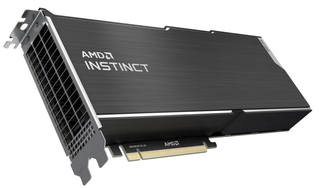
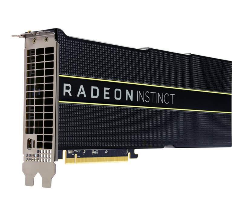
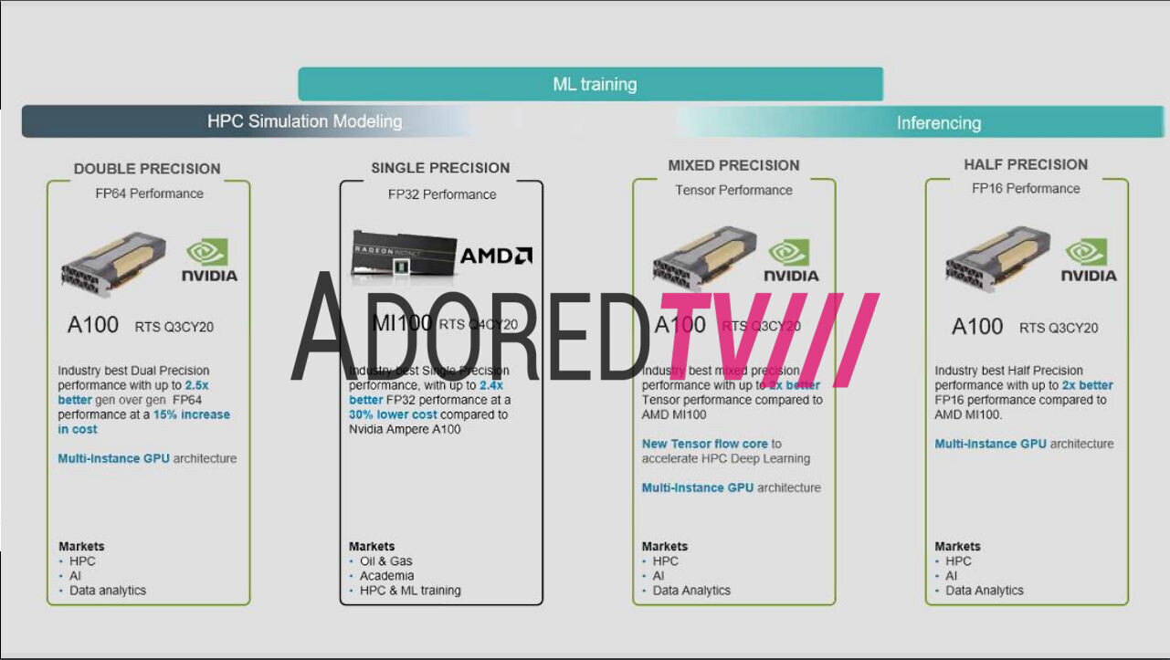
The U.S. Government has imposed restrictions on the export of AI compute GPUs to China and Russia without Government-authorization in the form of a waiver or a license. This impacts sales of products such as the NVIDIA A100, H100; AMD Instinct MI100, MI200; and the upcoming Intel "Ponte Vecchio," among others. The restrictions came to light when NVIDIA on Wednesday disclosed that it has received a Government notification about licensing requirements for export of its AI compute GPUs to Russia and China.

The notification doesn't specify the A100 and H100 by name, but defines AI inference performance thresholds to meet the licensing requirements. The Government wouldn't single out NVIDIA, and so competing products such as the AMD MI200 and the upcoming Intel Xe-HP "Ponte Vecchio" would fall within these restrictions. For NVIDIA, this is impacts $400 million in TAM, unless the Government licenses specific Russian and Chinese customers to purchase these GPUs from NVIDIA. Such trade restrictions usually come with riders to prevent resale or transshipment by companies outside the restricted region (eg: a distributor in a third waived country importing these chips in bulk and reselling them to these countries).

Tianshu Zhixin Big Island GPU is a 37 TeraFLOP FP32 Computing Monster

Tianshu Zhixin, a Chinese startup company dedicated to designing advanced processors for accelerating various kinds of tasks, has officially entered the production of its latest GPGPU design. Called "Big Island" GPU, it is the company's entry into the GPU market, currently dominated by AMD, NVIDIA, and soon Intel. So what is so special about Tianshu Zhixin's Big Island GPU, making it so important? Firstly, it represents China's attempt of independence from the outside processor suppliers, ensuring maximum security at all times. Secondly, it is an interesting feat to enter a market that is controlled by big players and attempt to grab a piece of that cake. To be successful, the GPU needs to represent a great design.

And great it is, at least on paper. The specifications list that Big Island is currently being manufactured on TSMC's 7 nm node using CoWoS packaging technology, enabling the die to feature over 24 billion transistors. When it comes to performance, the company claims that the GPU is capable of crunching 37 TeraFLOPs of single-precision FP32 data. At FP16/BF16 half-precision, the chip is capable of outputting 147 TeraFLOPs. When it comes to integer performance, it can achieve 317, 147, and 295 TOPS in INT32, INT16, and IN8 respectively. There is no data on double-precision floating-point numbers, so the chip is optimized for single-precision workloads. There is also 32 GB of HBM2 memory present, and it has 1.2 TB of bandwidth. If we compare the chip to the competing offers like NVIDIA A100 or AMD MI100, the new Big Island GPU outperforms both at single-precision FP32 compute tasks, for which it is designed.
Tianshu Zhixin Big Island Tianshu Zhixin Big Island Tianshu Zhixin Big Island Tianshu Zhixin Big Island
Pictures of possible solutions follow.

AMD Announces CDNA Architecture. Radeon MI100 is the World's Fastest HPC Accelerator

AMD today announced the new AMD Instinct MI100 accelerator - the world's fastest HPC GPU and the first x86 server GPU to surpass the 10 teraflops (FP64) performance barrier. Supported by new accelerated compute platforms from Dell, Gigabyte, HPE, and Supermicro, the MI100, combined with AMD EPYC CPUs and the ROCm 4.0 open software platform, is designed to propel new discoveries ahead of the exascale era.

Built on the new AMD CDNA architecture, the AMD Instinct MI100 GPU enables a new class of accelerated systems for HPC and AI when paired with 2nd Gen AMD EPYC processors. The MI100 offers up to 11.5 TFLOPS of peak FP64 performance for HPC and up to 46.1 TFLOPS peak FP32 Matrix performance for AI and machine learning workloads. With new AMD Matrix Core technology, the MI100 also delivers a nearly 7x boost in FP16 theoretical peak floating point performance for AI training workloads compared to AMD's prior generation accelerators.

AMD Eyes Mid-November CDNA Debut with Instinct MI100, "World's Fastest FP64 Accelerator"

AMD is eyeing a mid-November debut for its CDNA compute architecture with the Instinct MI100 compute accelerator card. CDNA is a fork of RDNA for headless GPU compute accelerators with large SIMD resources. An Aroged report pins the launch of the MI100 at November 16, 2020, according to leaked AMD documents it dug up. The Instinct MI100 will eye a slice of the same machine intelligence pie NVIDIA is seeking to dominate with its A100 Tensor Core compute accelerator.

It appears like the first MI100 cards will be built in the add-in-board form-factor with PCI-Express 4.0 x16 interfaces, although older reports do predict AMD creating a socketed variant of its Infinity Fabric interconnect for machines with larger numbers of these compute processors. In the leaked document, AMD claims that the Instinct MI100 is the "world's highest double-precision accelerator for machine learning, HPC, cloud compute, and rendering systems." This is an especially big claim given that the A100 Tensor Core features FP64 CUDA cores based on the "Ampere" architecture. Then again, given that AMD claims that the RDNA2 graphics architecture is clawing back at NVIDIA with performance at the high-end, the competitiveness of the Instinct MI100 against the A100 Tensor Core cannot be discounted.

AMD Radeon MI100 "Arcturus" Alleged Specification Listed, the GPU Could be Coming in December

AMD has been preparing to launch its MI100 accelerator and fight NVIDIA's A100 Ampere GPU in machine learning and AI horizon, and generally compute-intensive workloads. According to some news sources over at AdoredTV, the GPU alleged specifications were listed, along with some slides about the GPU which should be presented at the launch. So to start, this is what we have on the new Radeon MI100 "Arcturus" GPU based on CDNA architecture. The alleged specifications mention that the GPU will feature 120 Compute Units (CUs), meaning that if the GPU keeps the 64-core per CU configuration, we are looking at 7680 cores powered by CDNA architecture.

The leaked slide mentions that the GPU can put out as much as 42 TeraFLOPs of FP32, single-precision compute. This makes it more than twice as fast compared to NVIDIA's A100 GPU at FP32 workloads. To achieve that, the card would need to have all of its 7680 cores running at 2.75 GHz, which would be a bit high number. On the same slide, the GPU is claimed to have 9.5 TeraFLOPs of FP64 dual-precision performance, while the FP16 power is going to be around 150 TeraFLOPs. For comparison, the A100 GPU from NVIDIA features 9.7 TeraFLOPS of FP64, 19.5 TeraFLOPS of FP32, and 312 (or 634 with sparsity enabled) TeraFLOPs of FP16 compute. AMD GPU is allegedly only more powerful for FP32 workloads, where it outperforms the NVIDIA card by 2.4 times. And if that is really the case, AMD has found its niche in the HPC sector, and it plans to dominate there. According to AdoredTV sources, the GPU could be coming in December of this year.

AMD's Next-Generation Radeon Instinct "Arcturus" Test Board Features 120 CUs

AMD is preparing to launch its next-generation of Radeon Instinct GPUs based on the new CDNA architecture designed for enterprise deployments. Thanks to the popular hardware leaker _rogame (@_rogame) we have some information about the configuration of the upcoming Radeon Instinct MI100 "Arcturus" server GPU. Previously, we obtained the BIOS of the Arcturus GPU that showed a configuration of 128 Compute Units (CUs), which resulted in 8,192 of CDNA cores. That configuration had a specific setup of 1334 MHz GPU clock, SoC frequency of 1091 MHz, and memory speed of 1000 MHz. However, there was another GPU test board spotted which featured a bit different specification.

The reported configuration is an Arcturus GPU with 120 CUs, resulting in a CDNA core count of 7,680 cores. These cores are running at frequencies of 878 MHz for the core clock, 750 MHz SoC clock, and a surprising 1200 MHz memory clock. While the SoC and core clocks are lower than the previous report, along with the CU count, the memory clock is up by 200 MHz. It is important to note that this is just a test board/variation of the MI100, and actual frequencies should be different.
AMD Radeon Instinct MI60

AMD Radeon Instinct MI100 "Arcturus" Hits the Radar, We Have its BIOS

AMD's upcoming large post-Navi graphics chip, codenamed "Arcturus," will debut as "Radeon Instinct MI100", which is an AI-ML accelerator under the Radeon Instinct brand, which AMD calls "Server Accelerators." TechPowerUp accessed its BIOS, which is now up on our VGA BIOS database. The card goes with the device ID "0x1002 0x738C," which confirms "AMD" and "Arcturus,". The BIOS also confirms that memory size is at a massive 32 GB HBM2, clocked at 1000 MHz real (possibly 1 TB/s bandwidth, if memory bus width is 4096-bit).

Both Samsung (KHA884901X) and Hynix memory (H5VR64ESA8H) is supported, which is an important capability for AMD's supply chain. From the ID string "MI100 D34303 A1 XL 200W 32GB 1000m" we can derive that the TDP limit is set to a surprisingly low 200 W, especially considering this is a 128 CU / 8,192 shader count design. Vega 64 and Radeon Instinct MI60 for comparison have around 300 W power budget with 4,096 shaders, 5700 XT has 225 W with 2560 shaders, so either AMD achieved some monumental efficiency improvements with Arcturus or the whole design is intentionally running constrained, so that AMD doesn't reveal their hand to these partners, doing early testing of the card.
Return to Keyword Browsing
Jun 11th, 2024 18:58 EDT change timezone

New Forum Posts

Popular Reviews

Controversial News Posts