News Posts matching #R&D

Return to Keyword Browsing

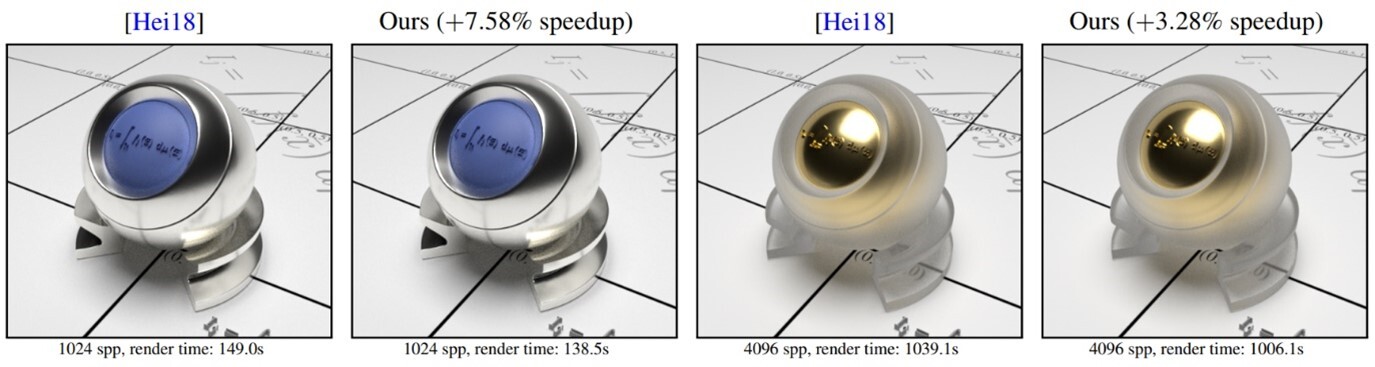
SK hynix Signs Investment Agreement of Advanced Chip Packaging with Indiana

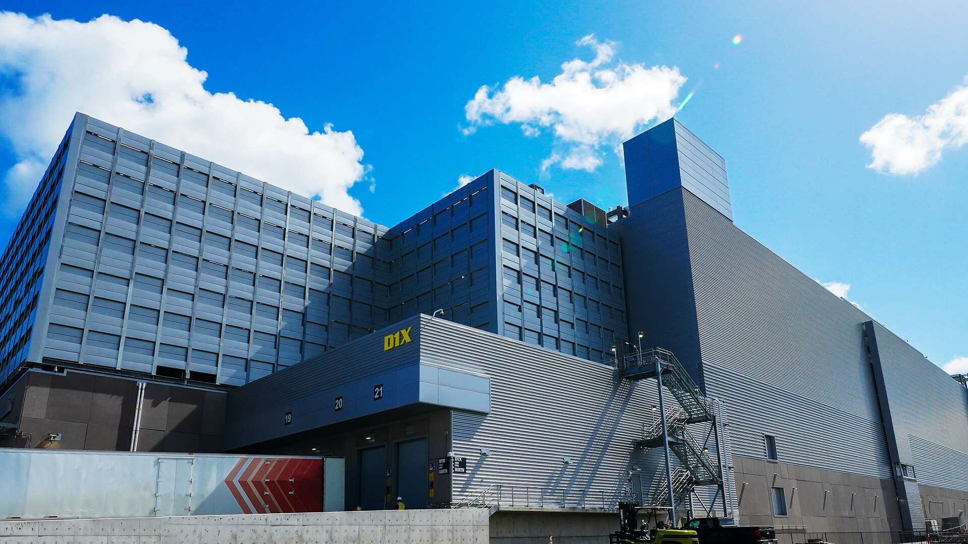
SK hynix Inc., the world's leading producer of High-Bandwidth Memory (HBM) chips, announced today that it will invest an estimated $3.87 billion in West Lafayette, Indiana to build an advanced packaging fabrication and R&D facility for AI products. The project, the first of its kind in the United States, is expected to drive innovation in the nation's AI supply chain, while bringing more than a thousand new jobs to the region.

The company held an investment agreement ceremony with officials from Indiana State, Purdue University, and the U.S. government at Purdue University in West Lafayette on the 3rd and officially announced the plan. At the event, officials from each party including Governor of Indiana Eric Holcomb, Senator Todd Young, Director of the White House Office of Science and Technology Policy Arati Prabhakar, Assistant Secretary of Commerce Arun Venkataraman, Secretary of Commerce State of Indiana David Rosenberg, Purdue University President Mung Chiang, Chairman of Purdue Research Foundation Mitch Daniels, Mayor of city of West Lafayette Erin Easter, Ambassador of the Republic of Korea to the United States Hyundong Cho, Consul General of the Republic of Korea in Chicago Junghan Kim, SK vice chairman Jeong Joon Yu, SK hynix CEO Kwak Noh-Jung and SK hynix Head of Package & Test Choi Woojin, participated.

Ubisoft Exploring Generative AI, Could Revolutionize NPC Narratives

Have you ever dreamed of having a real conversation with an NPC in a video game? Not just one gated within a dialogue tree of pre-determined answers, but an actual conversation, conducted through spontaneous action and reaction? Lately, a small R&D team at Ubisoft's Paris studio, in collaboration with Nvidia's Audio2Face application and Inworld's Large Language Model (LLM), have been experimenting with generative AI in an attempt to turn this dream into a reality. Their project, NEO NPC, uses GenAI to prod at the limits of how a player can interact with an NPC without breaking the authenticity of the situation they are in, or the character of the NPC itself.

Considering that word—authenticity—the project has had to be a hugely collaborative effort across artistic and scientific disciplines. Generative AI is a hot topic of conversation in the videogame industry, and Senior Vice President of Production Technology Guillemette Picard is keen to stress that the goal behind all genAI projects at Ubisoft is to bring value to the player; and that means continuing to focus on human creativity behind the scenes. "The way we worked on this project, is always with our players and our developers in mind," says Picard. "With the player in mind, we know that developers and their creativity must still drive our projects. Generative AI is only of value if it has value for them."

Arizona State University and Deca Technologies to Pioneer North America's First R&D Center for Advanced Fan-Out Wafer-Level Packaging

Arizona State University (ASU) and Deca Technologies (Deca), a premier provider of advanced wafer- and panel-level packaging technology, today announced a groundbreaking collaboration to create North America's first fan-out wafer-level packaging (FOWLP) research and development center.

The new Center for Advanced Wafer-Level Packaging Applications and Development is set to catalyze innovation in the United States, expanding domestic semiconductor manufacturing capabilities and driving advancements in cutting-edge fields such as artificial intelligence, machine learning, automotive electronics and high-performance computing.

Extropic Intends to Accelerate AI through Thermodynamic Computing

Extropic, a pioneer in physics-based computing, this week emerged from stealth mode and announced the release of its Litepaper, which outlines the company's revolutionary approach to AI acceleration through thermodynamic computing. Founded in 2022 by Guillaume Verdon, Extropic has been developing novel chips and algorithms that leverage the natural properties of out-of-equilibrium thermodynamic systems to perform probabilistic computations for generative AI applications in a highly efficient manner. The Litepaper delves into Extropic's groundbreaking computational paradigm, which aims to address the limitations of current digital hardware in handling the complex probability distributions required for generative AI.

Today's algorithms spend around 25% of their time moving numbers around in memory, limiting the speedup achievable by accelerating specific operations. In contrast, Extropic's chips natively accelerate a broad class of probabilistic algorithms by running them physically as a rapid and energy-efficient, physics-based process in their entirety, unlocking a new regime of AI acceleration well beyond what was previously thought achievable. In coming out of stealth, the company has announced the fabrication of a superconducting prototype processor and developments surrounding room-temperature semiconductor-based devices for the broader market, with the goal of revolutionizing the field of AI acceleration and enabling new possibilities in generative AI.

The SEA Projects Prepare Europe for Exascale Supercomputing

The HPC research projects DEEP-SEA, IO-SEA and RED-SEA are wrapping up this month after a three-year project term. The three projects worked together to develop key technologies for European Exascale supercomputers, based on the Modular Supercomputing Architecture (MSA), a blueprint architecture for highly efficient and scalable heterogeneous Exascale HPC systems. To achieve this, the three projects collaborated on system software and programming environments, data management and storage, as well as interconnects adapted to this architecture. The results of their joint work will be presented at a co-design workshop and poster session at the EuroHPC Summit (Antwerp, 18-21 March, www.eurohpcsummit.eu).

Samsung Accelerates R&D of Glass Substrate Chip Packaging

The Samsung Group has formed a new cross-department alliance—according to South Korea's Sedaily—this joint operation will concentrate on the research and development of a "dream substrate." The company's Electronics, Electrical Engineering, and Display divisions are collaborating in order to accelerate commercialization of "glass substrate" chip packaging. Last September, Intel revealed its intention to become an industry leader in "glass substrate production for next-generation advanced packaging." Team Blue's shiny new Arizona fabrication site will be taking on this challenge, following ten years of internal R&D work. Industry watchdogs reckon that mass production—in North America—is not expected to kick off anytime soon. Sensible guesstimates suggest a start date somewhere in 2030.

The Sedaily article states that Samsung's triple department alliance will target "commercialization faster than Intel." Company representatives—in attendance at CES 2024—set a 2026 window as their commencement goal for advanced glass substrate chip package mass production. An unnamed South Korean industry watcher has welcomed a new entrant on the field: "as each company possesses the world's best technology, synergies will be maximized in glass substrate research, which is a promising field...it is also important to watch how the glass substrate ecosystem of Samsung's joint venture will be established." Glass substrate packaging is ideal for "large-area and high-performance chip combinations" due to inherent heat-resistant properties and material strength. So far, the semiconductor industry has struggled with its development—hence the continued reliance on plastic boards and organic materials.

Helldivers 2 Warbond System Previewed Ahead of March 14 Launch

Helldivers, get the Cutting Edge advantage on the battlefield! Greetings, fearless heroes of galactic democracy! Steel yourself for the next big push against the disgraceful enemies of freedom with our brand-new Warbond—Cutting Edge! Packed with high-voltage vibes, Cutting Edge gives you the chance to enhance your loadout of liberty with ultra-futuristic armour, guns that spit lightning, super stylish capes and epic emotes.

Super Earth R&D Experiments
Helldivers… we need your help. The brainiacs in Super Earth Research & Development have some cool experimental armour ready to be field-tested. This is where you come in, you're just the right people for the job.

3D Nanoscale Petabit Capacity Optical Disk Format Proposed by Chinese R&D Teams

The University of Shanghai for Science and Technology (USST), Peking University and the Shanghai Institute of Optics and Fine Mechanics (SIOM) are collaborating on new Optical Data Storage (ODS) technologies—a recently published paper reveals that scientists are attempting to create 3D nanoscale optical disk memory that breaks into petabit capacities. Society (as a whole) has an ever-growing data demand—this requires the development of improved high-capacity storage technologies—the R&D teams believe that ODS presents a viable alternative route to traditional present day solutions: "data centers based on major storage technologies such as semiconductor flash devices and hard disk drives have high energy burdens, high operation costs and short lifespans."

The proposed ODS format could be a "promising solution for cost-effective long-term archival data storage." The researchers note that current (e.g Blu-ray) and previous generation ODS technologies have been: "limited by low capacities and the challenge of increasing areal density." In order to get ODS up to petabit capacity levels, several innovations are required—the Nature.com abstract stated: "extending the planar recording architecture to three dimensions with hundreds of layers, meanwhile breaking the optical diffraction limit barrier of the recorded spots. We develop an optical recording medium based on a photoresist film doped with aggregation-induced emission dye, which can be optically stimulated by femtosecond laser beams. This film is highly transparent and uniform, and the aggregation-induced emission phenomenon provides the storage mechanism. It can also be inhibited by another deactivating beam, resulting in a recording spot with a super-resolution scale." The novel optical storage medium relies on dye-doped photoresist (DDPR) with aggregation-induced emission luminogens (AIE-DDPR)—a 515 nm femtosecond Gaussian laser beam takes care of optical writing tasks, while a doughnut-shaped 639 nm continuous wave laser beam is tasked with retrieval. A 480 nm pulsed laser and a 592 nm continuous wave laser work in tandem to read data.

Samsung & Vodafone "Open RAN Ecosystem" Bolstered by AMD EPYC 8004 Series

Samsung Electronics and Vodafone, in collaboration with AMD, today announced that the three companies have successfully demonstrated an end-to-end call with the latest AMD processors enabling Open RAN technology, a first for the industry. This joint achievement represents the companies' technical leadership in enriching the Open RAN ecosystem throughout the industry. Conducted in Samsung's R&D lab in Korea, the first call was completed using Samsung's versatile, O-RAN-compliant, virtualized RAN (vRAN) software, powered by AMD EPYC 8004 Series processors on Supermicro's Telco/Edge servers, supported by Wind River Studio Container-as-a-Service (CaaS) platform. This demonstration aimed to verify optimized performance, energy efficiency and interoperability among partners' solutions.

The joint demonstration represents Samsung and Vodafone's ongoing commitment to reinforce their position in the Open RAN market and expand their ecosystem with industry-leading partners. This broader and growing Open RAN ecosystem helps operators to build and modernize mobile networks with greater flexibility, faster time-to-market (TTM), and unmatched performance. "Open RAN represents the forthcoming major transformation in advancing mobile networks for the future. Reaching this milestone with top industry partners like Samsung and AMD shows Vodafone's dedication to delivering on the promise of Open RAN innovation," said Nadia Benabdallah, Network Strategy and Engineering Director at Vodafone Group. "Vodafone is continually looking to innovate its network by exploring the potential and diversity of the ecosystem."

U.S. CHIPS Act Outlines $500 Million Fund for Research Institutes & Packaging Tech Development

Yesterday, the U.S. Department of Commerce publicly announced two new notices of intent—as reported by Tom's Hardware, this involves the latest distributions from the CHIPS Act's $11 billion R&D budget: "$300 million is to be made available across multiple awards of up to $100 million (not including voluntary co-investment) for research on advanced packaging, while another $200 million (or more) is set aside to create the CHIPS Manufacturing USA Institute. Companies will have to compete for the funds by filing an application." The Act's primary $39 billion tranche is designated to new construction endeavors, e.g. the founding of manufacturing facilities.

A grand total of $52 billion was set aside for the CHIPS Act in 2022, which immediately attracted the attention of several semiconductor industry giants. Companies with headquarters outside of North America were allowed to send in applications. Last year, Intel CEO Pat Gelsinger, made some controversial statements regarding his company's worthiness of government funding. In his opinion, Team Blue is due the "lion's share" due to his operation being a USA firm—the likes of TSMC and Samsung are far less deserving of subsidies.

EdgeCortix Foresees Barrier Breaking Efficient Next-gen Edge AI Chips

EdgeCortix, the Japan-based fabless semiconductor company focused on energy-efficient AI processing, predicts that 2024 is set to be a watershed moment for Edge AI. Through its predictions for the year, EdgeCortix believes that Edge AI landscape will be transformed during this exciting year for the industry. Next-gen AI chips, hybrid edge-cloud architectures, software supremacy and the rise of new generative-AI applications "at the edge," will revolutionize the world of business as we know it.

1. Next-Gen efficient Edge AI Chips will break barriers:
Prepare for a hardware uprising! EdgeCortix foresees next-gen energy-efficient AI chips that not only break the barriers of processing power but redefine them. These chips are not just powerful; they are customized for multi-modal generative AI and efficient language models, enabling cutting-edge AI capabilities at low power for a whole new spectrum of applications.

Synopsys to Acquire Ansys, Creating a Leader in Silicon to Systems Design Solutions

Synopsys (NASDAQ: SNPS) and Ansys (NASDAQ: ANSS) today announced that they have entered into a definitive agreement under which Synopsys will acquire Ansys. Under the terms of the agreement, Ansys shareholders will receive $197.00 in cash and 0.3450 shares of Synopsys common stock for each Ansys share, representing an enterprise value of approximately $35 billion based on the closing price of Synopsys common stock on December 21, 2023. Bringing together Synopsys' pioneering semiconductor electronic design automation (EDA) with Ansys' broad simulation and analysis portfolio will create a leader in silicon to systems design solutions.

"The megatrends of AI, silicon proliferation and software-defined systems are requiring more compute performance and efficiency in the face of growing, systemic complexity. Bringing together Synopsys' industry-leading EDA solutions with Ansys' world-class simulation and analysis capabilities will enable us to deliver a holistic, powerful and seamlessly integrated silicon to systems approach to innovation to help maximize the capabilities of technology R&D teams across a broad range of industries," said Sassine Ghazi, President and CEO of Synopsys. "This is the logical next step for our successful, seven-year partnership with Ansys and I look forward to working closely with Ajei and the talented Ansys team to realize the benefits of this combination for our customers, shareholders and employees."

TCL CSOT Unveils Latest IJP OLED & FMM-OLED Tech

TCL CSOT, a renowned industry player developing advanced, innovative display technologies, recently showcased its extensive range of products spanning automobiles, laptops, tablets, smartphones, TVs, VR, and more at CES 2024. Among its showcased offering, the company's cutting-edge OLED and MLED technologies, notably its Inkjet Printing OLED (IJP OLED) and Fine Metal Mask-OLED (FMM-OLED) display technologies, drew major attention from the public.

Industry Breakthroughs in IJP OLED Technology
Over the years, TCL CSOT has been actively laying the groundwork for adopting inkjet-printing technology to manufacture OLED displays. This IJP OLED technology brings advantages including a wider color gamut, higher resolution, greater material utilization efficiency, lower power consumption, and reduced operating costs. TCL CSOT is currently focusing on medium and large-sized products for Inkjet Printing OLED, such as TVs, and aims to accelerate the industrialization by also including medium-sized screens, such as laptops and vehicles. In addition to focusing on medium and large-sized products, TCL CSOT aims to achieve mass production of IJP OLED in a small scale, particularly in the medical and IT fields, in 2024.

Intel Announces New Investments for Gordon Moore Park R&D Facilities in Oregon

Intel today shared its plans to advance its semiconductor technology development facilities at the Gordon Moore Park at Ronler Acres in Hillsboro, Oregon. The campus is Intel's innovation hub for leading-edge semiconductor research, technology development and manufacturing in the United States. This undertaking is possible with support from the state of Oregon, city of Hillsboro and Washington County, and in anticipation of support from the U.S. CHIPS and Science Act.

"Intel has been dedicated to driving innovation and advancing technology in Oregon for almost five decades, and we are set to lead the charge in restoring America's leadership in semiconductor R&D and manufacturing, backed by Oregon and the U.S. CHIPS Act. This investment further solidifies our commitment to the Silicon Forest and rebalancing the global semiconductor supply chain," said Dr. Ann Kelleher, Intel executive vice president and general manager of the Technology Development Group.

TSMC, Broadcom & NVIDIA Alliance Reportedly Set to Advance Silicon Photonics R&D

Taiwan's Economic Daily reckons that a freshly formed partnership between TSMC, Broadcom, and NVIDIA will result in the development of cutting-edge silicon photonics. The likes of IBM, Intel and various academic institutes are already deep into their own research and development processes, but the alleged new alliance is said to focus on advancing AI computer hardware. The report cites a significant allocation of—roughly 200—TSMC staffers onto R&D involving the integration of silicon photonic technologies into high performance computing (HPC) solutions. They are very likely hoping that the usage of optical interconnects (on a silicon medium) will result in greater data transfer rates between and within microchips. Other benefits include longer transmission distances and a lower consumption of power.

TSMC vice president Yu Zhenhua has placed emphasis on innovation, in a similar fashion to his boss, within the development process (industry-wide): "If we can provide a good silicon photonics integrated system, we can solve the two key issues of energy efficiency and AI computing power. This will be a new one...Paradigm shift. We may be at the beginning of a new era." The firm is facing unprecedented demand from its clients—it hopes to further expand its advanced chip packaging capacity to address these issues by late 2024. A shift away from the limitations of "conventional electric" data transmissions could bring next generation AI compute GPUs onto the market by 2025.

IDC Forecasts Worldwide Quantum Computing Market to Grow to $7.6 Billion in 2027

International Data Corporation (IDC) today published its second forecast for the worldwide quantum computing market, projecting customer spend for quantum computing to grow from $1.1 billion in 2022 to $7.6 billion in 2027. This represents a five-year compound annual growth rate (CAGR) of 48.1%. The forecast includes base quantum computing as a service as well as enabling and adjacent quantum computing as a service.

The new forecast is considerably lower than IDC's previous quantum computing forecast, which was published in 2021. In the interim, customer spend for quantum computing has been negatively impacted by several factors, including: slower than expected advances in quantum hardware development, which have delayed potential return on investment; the emergence of other technologies such as generative AI, which are expected to offer greater near-term value for end users; and an array of macroeconomic factors, such as higher interest and inflation rates and the prospect of an economic recession.

TSMC Inaugurates Global R&D Center, Celebrating Its Newest Hub for Technology Innovation

TSMC today held an inauguration ceremony for its global Research and Development Center in Hsinchu, Taiwan, celebrating the Company's newest hub for bringing the next generations of semiconductor technology into reality with customers, R&D partners in industry and academia, design ecosystem partners, and senior government leaders.

The R&D Center will serve as the new home for TSMC's R&D Organization, including the researchers who will develop TSMC's leading-edge process technology at the 2-nanometer generation and beyond, as well as scientists and scholars blazing the trail with exploratory research into fields such as novel materials and transistor structures. With R&D employees already relocating to their workplaces in the new building, it will be ready for its full complement of more than 7,000 staff by September 2023.

AMD Announces Plan to Invest Approximately $400 Million Over the Next Five Years in India

AMD today announced plans for continued growth in India through an approximate $400M investment over the next five years. The planned investment includes a new AMD campus in Bangalore, Karnataka that will serve as the company's largest design center, as well as the addition of approximately 3,000 new engineering roles by the end of 2028. The new AMD campus is expected to open before the end of 2023 and will feature extensive lab space, state-of-the-art collaboration tools and seating configurations designed to foster teamwork. The investment is supported by the various policy initiatives of the Government of India focused on the semiconductor industry.

"We welcome the AMD plan to expand its leading-edge R&D engineering operations in India," said Mr. Ashwini Vaishnaw, Union Cabinet Minister for Railways, Telecommunications, Electronics and Information Technology, Government of India. "I welcome AMD's decision to set up its largest R&D design center in India and expansion of the India-AMD partnership. It will certainly play an important role in building a world class semiconductor design and innovation ecosystem. It will also provide tremendous opportunities for our large pool of highly skilled semiconductor engineers and researchers and will catalyse PM Narendra Modi's vision of India becoming a global talent hub," said Mr. Rajeev Chandrasekhar, Minister of State for Electronics and IT, Skill Development and Entrepreneurship.

NVIDIA Espouses Generative AI for Improved Productivity Across Industries

A watershed moment on Nov. 22, 2022, was mostly virtual, yet it shook the foundations of nearly every industry on the planet. On that day, OpenAI released ChatGPT, the most advanced artificial intelligence chatbot ever developed. This set off demand for generative AI applications that help businesses become more efficient, from providing consumers with answers to their questions to accelerating the work of researchers as they seek scientific breakthroughs, and much, much more.

Businesses that previously dabbled in AI are now rushing to adopt and deploy the latest applications. Generative AI—the ability of algorithms to create new text, images, sounds, animations, 3D models and even computer code—is moving at warp speed, transforming the way people work and play. By employing large language models (LLMs) to handle queries, the technology can dramatically reduce the time people devote to manual tasks like searching for and compiling information.

NVIDIA DRIVE Orin SoC Key Component in XPENG G6 Coupe SUV

China electric vehicle maker XPENG Motors has announced its new G6 coupe SUV—featuring an NVIDIA-powered intelligent advanced driver assistance system—is now available to the China market. The G6 is XPENG's first model featuring the company's proprietary Smart Electric Platform Architecture (SEPA) 2.0, which aims to reduce development and manufacturing costs and shorten R&D cycles since the modular architecture will be compatible with future models.

The electric SUV also features the XPENG Navigation Guided Pilot (XNGP), a full scenario-based intelligent assisted driving system. It's powered by the cutting-edge NVIDIA DRIVE Orin compute and XPENG's full-stack software developed in-house. The XNGP system first made its debut in the EV maker's flagship G9 SUV, touting a safe, reliable, advanced driving experience behind the wheel.

Jensen Huang & Leading EU Generative AI Execs Participated in Fireside Chat

Three leading European generative AI startups joined NVIDIA founder and CEO Jensen Huang this week to talk about the new era of computing. More than 500 developers, researchers, entrepreneurs and executives from across Europe and further afield packed into the Spindler and Klatt, a sleek, riverside gathering spot in Berlin. Huang started the reception by touching on the message he delivered Monday at the Berlin Summit for Earth Virtualization Engines (EVE), an international collaboration focused on climate science. He shared details of NVIDIA's Earth-2 initiative and how accelerated computing, AI-augmented simulation and interactive digital twins drive climate science research.

Before sitting down for a fireside chat with the founders of the three startups, Huang introduced some "special guests" to the audience—four of the world's leading climate modeling scientists, who he called the "unsung heroes" of saving the planet. "These scientists have dedicated their careers to advancing climate science," said Huang. "With the vision of EVE, they are the architects of the new era of climate science."

Intel Developing Efficient Solution for Path Tracing on Integrated GPUs

Intel's software engineers are working on path-traced light simulation and conducting neural graphics research, as documented in a recent company news article, with an ambition to create a more efficient solution for integrated graphics cards. The company's Graphics Research Organization is set to present their path-traced optimizations at SIGGRAPH 2023. Their papers have been showcased at recent EGSR and HPG events. The team is aiming to get iGPUs running path-tracing in real time, by reducing the number of calculations required to simulate light bounces.

The article covers three different techniques, all designed to improve GPU performance: "Across the process of path tracing, the research presented in these papers demonstrates improvements in efficiency in path tracing's main building blocks, namely ray tracing, shading, and sampling. These are important components to make photorealistic rendering with path tracing available on more affordable GPUs, such as Intel Arc GPUs, and a step toward real-time performance on integrated GPUs." Although there is an emphasis on in-house products in the article, Intel's "open source-first mindset" hints that their R&D could be shared with others—NVIDIA and AMD are likely still struggling to make ray tracing practical on their modest graphics card models.

Huawei Launching Commercial 5.5G Network Equipment in 2024

Huawei announced they will launch a complete set of commercial 5.5G network equipment in 2024 at the 5G Advanced Forum during MWC Shanghai 2023. Huawei's Director and President of ICT Products & Solutions Yang Chaobin who made the announcement said the company intends for this launch to mark the beginning of the 5.5G era for the ICT industry.

5G deployment progressed rapidly over the past four years and is already yielding significant financial gains. Today, there are more than 260 commercial 5G networks worldwide, serving over 1.2 billion users, and there are already 115 million gigabit F5G users. With service models and content continuously evolving, breakthroughs in technologies like glasses-free 3D are creating unprecedented immersive experiences for users. However, these new services continue to require stronger 5G network capabilities. The industry has widely agreed that 5.5G will be a key milestone in 5G evolution, and that it is fast approaching.

RPI Announced as the First University to House IBM's Quantum System One

Today, it was announced that Rensselaer Polytechnic Institute will become the first university in the world to house an IBM Quantum System One. The IBM quantum computer, intended to be operational by January of 2024, will serve as the foundation of a new IBM Quantum Computational Center in partnership with Rensselaer Polytechnic Institute (RPI). By partnering, RPI's vision is to greatly enhance the educational experiences and research capabilities of students and researchers at RPI and other institutions, propel the Capital Region into a top location for talent, and accelerate New York's growth as a technology epicenter.

RPI's advance into research of applications for quantum computing will represent a more than $150 million investment once fully realized, aided by philanthropic support from Curtis R. Priem '82, vice chair of RPI's Board of Trustees. The new quantum computer will be part of RPI's new Curtis Priem Quantum Constellation, a faculty endowed center for collaborative research, which will prioritize the hiring of additional faculty leaders who will leverage the quantum computing system.

TSMC Said to Start Construction of 1.4 nm Fab in 2026

According to Taiwanese media, TSMC will start production of its first 1.4 nm fab in 2026, with chip production in the fab said to start sometime in 2027 or 2028. The new fab will be located in Longtan Science Park outside of Hsinchu in Taiwan, where many of TSMC's current fabs are located. TSMC is currently constructing a 2 nm and below node R&D facility at a nearby plot of land to where the new fab is expected to be built. This facility is expected to be finished in 2025 and TSMC has been allocated a total area of just over 158 hectares of land for future expansion in the area.

In related news, TSMC is expected to be charging US$25,000 per 2 nm GAA wafer, which is an increase of about a fifth compared to its 3 nm wafers which are going for around US$20,000. This is largely due to the nodes being fully booked and TSMC being able to charge a premium for its cutting edge nodes. TSMC is also expanding in CoWoS packaging facilities due to increased demand from both AMD and NVIDIA for AI related products. Currently TSMC is said to be able to output 12,000 CoWoS wafers per month and this is twice as much as last year, yet TSMC is unable to meet demand from its customers.
Return to Keyword Browsing
Apr 29th, 2024 18:39 EDT change timezone

New Forum Posts

Popular Reviews

Controversial News Posts