News Posts matching #Sandy Bridge-E

Return to Keyword Browsing

Intel Core i7 "Broadwell-E" HEDT Chips Arrive in 2016

Intel is beginning to put out the first details of its next high-end desktop (HEDT) processors, internally. Codenamed "Broadwell-E," the company's next Core i7 HEDT chips will be built in the existing LGA2011v3 package, and will be compatible with existing motherboards based on Intel's X99 Express chipset (with BIOS updates). Much like "Ivy Bridge-E" was to "Sandy Bridge-E," these chips will introduce only incremental updates, and nothing major, in terms of architecture.

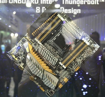
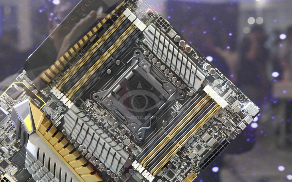
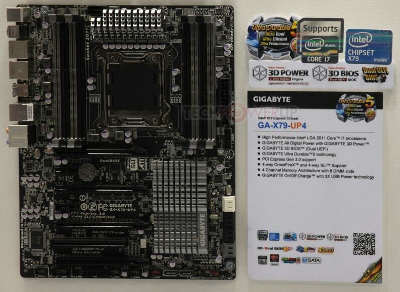
To begin with, Core i7 "Broadwell-E" will be built in the 14 nanometer silicon fab process, and will feature 6 to 8 cores based on the "Broadwell" micro-architecture. These cores will be cushioned with up to 20 MB of L3 cache. The chip is pin-compatible to "Haswell-E," and so its I/O will be identical, featuring a quad-channel DDR4 integrated memory controller. One difference is that Intel may can the 28-lane PCIe approach with the entry-level part; or at least it doesn't find mention on the slide. If it's true, all parts based on this silicon, will feature 40-lane PCIe interfaces. The TDP of these chips will be rated at 140W. Intel is expected to launch the Core i7 "Broadwell-E" in 2016.

Ivy Bridge-E Not a Cut-down 8-core, 20 MB LLC Die

Unlike Core i7 "Sandy Bridge-E," chips, which were quad-core or six-core parts cut-down from a common silicon shared with Xeon "Sandy Bridge-EP," which physically features eight cores and 20 MB of L3 cache; the upcoming Core i7 "Ivy Bridge-E" is based on a silicon that physically features just six cores, and 15 MB (or maybe 16 MB) of L3 cache. On the Core i7-4960X Extreme Edition, practically no component on the die is disabled. The Core i7-4930K features just 12 MB of L3 cache, while the Core i7-4820K features two out of six cores disabled, and just 10 MB of L3 cache.

"Ivy Bridge-E" is a variant of one of three large 22 nm dies Intel designed, based on the "Ivy Bridge" micro-architecture, next to a 10-core die with 25 MB of L3 cache, and a 12-core die with 30 MB of L3 cache. Aside from up to six cores, "Ivy Bridge-E" features a PCI-Express gen 3.0 certified root-complex (certified in way that NVIDIA would approve of), and a quad-channel (256-bit wide) DDR3 integrated memory controller, with native support for DDR3-1866. Intel's Core i7 "Ivy Bridge-E" series should launch on or before the 10th of September. Parts in the series will run on existing socket LGA2011 motherboards, with a BIOS update.

Curious-looking Core i7-3910K LGA2011 Processor Surfaces

Intel's Core i7 "Ivy Bridge-E" series may be less than two months away from seeing the light of the day, but in the run up to that, a curious-looking Core i7-3910K "Sandy Bridge-E" part cropped up on roadmaps with retailers. We're pretty sure it's not a typo misread by someone for "i7-3970X," because the list even mentions the S-spec code "SR0TN," which doesn't correspond with the "SR0WR" s-spec code of the i7-3970X.

The Core i7-3910K is based on the same Sandy Bridge-E C2-stepping silicon as the i7-3970X, and is said to feature 3.00 GHz clock speed. There's no clarity on exactly how many cores it features, but given that it's named in the i7-3900 series, and not the i7-3800 series, we're leaning toward it being a six-core part. A bid by Intel to clear out "imperfect" Sandy Bridge-E silicon by giving it a relatively low clock speed? We doubt that, it features the "K" brand extension, which denotes unlocked base-clock multiplier. Intel's cheapest LGA2011 six-core part is the i7-3930K, which goes for roughly US $550. If Intel prices this chip just right, by that we mean $400-ish, it could be a tease for all those shelling out $350 for a Core i7-4770K. Low clock speed, but unlocked. Two extra cores, quad-channel memory, and a bigger PCIe budget, albeit an older micro-architecture. Decisions, decisions.

Intel Core i7 "Ivy Bridge-E" and Core i3 "Haswell" Series Detailed

We know from older reports that Intel will refresh its socket LGA2011 HEDT (high-end desktop) product family with three new parts, based on the new 22 nm "Ivy Bridge-E" silicon. A table detailing their clock speeds was leaked to the web. In addition, we got details of what Intel's entry-level Core i3 "Haswell" line of dual-core processors would look like, specs-wise. The Ivy Bridge-E silicon, is to a large part an optical shrink of the Sandy Bridge-E silicon, with a few improvements. The chip is fabricated on Intel's 22 nm node with tri-gate transistors, the IMC natively supports DDR3-1866 MHz, the PCI-Express root complex is gen 3.0 certified, and the CPUID features the new RdRAND instruction set. Aside from these clock speeds are increased across the board, although TDP isn't lowered from the previous 130W.

Leading the Core i7 "Ivy Bridge-E" pack is the Core i7-4960X Extreme Edition, with its 3.60 GHz core, 4.00 GHz maximum Turbo Boost, unlocked base-clock multiplier, and 15 MB L3 cache. This six-core chip will command a four-figure price. Next up, is the Core i7-4930K, with 3.40 GHz core, 3.90 GHz maximum Turbo Boost, unlocked base-clock multiplier, and 12 MB L3 cache. This chip could be 30-40 percent cheaper than the i7-4960X. The cheapest of the lot, though, is the Core i7-4820K. This quad-core part, interestingly, features unlocked base-clock multiplier, unlike its predecessor, the i7-3820. Perhaps Intel didn't want a repeat of Core i7-3770K cannibalizing the i7-3820. The i7-4820K features 3.70 GHz core, 3.90 GHz Turbo Boost, and 10 MB of L3 cache. The chip may be priced in the same range as the i7-4770K. All three parts feature quad-channel DDR3 integrated memory controllers, with native support for DDR3-1866.

Core i7-4960X "Ivy Bridge-E" Roughly 10% Faster than i7-3970X: Early Tests

PC enthusiast "Toppc" with the Coolaler.com, with access to a Core i7 "Ivy Bridge-E" sample clocked to match specifications of the Core i7-4960X, wasted no time in comparing the chip to a Core i7-3970X "Sandy Bridge-E." The two chips share a common socket LGA2011 design, and run on motherboards with Intel X79 Express chipset. An MSI X79A-GD45 Plus, with V17.1 BIOS was used to run the two chips. Among the tests Toppc put the chip through, are overclocker favorites SuperPi mod 1.6, CPU Mark '99, WPrime 1.63, Cinebench 11.5, 3DMark Vantage (CPU score), and 3DMark 06 (CPU score).

The Ivy Bridge-E chip outperformed its predecessor by roughly 5-10 percent across the board. In Cinebench, the i7-4960X scored 10.94 points in comparison to the i7-3970X' 10.16; SuperPi 32M was crunched by the i7-4960X in 9m 22.6s compared to the 9m 55.4s of the i7-3970X; CPU Mark scores between the two are 561 vs. 533, respectively; 3DMark Vantage CPU score being 38,644 points vs. 35,804, respectively; and 3DMark 06 scores 8,586 points vs. 8,099 points, respectively. In WPrime, the i7-4960X crunched 32M in 4.601s, compared to its predecessor's 5.01s. Below are the test screenshots, please note that they're high-resolution images, so please open each in a new tab.

Intel Core "Haswell" Easier to Overclock

At the Intel Developer Forum (IDF) 2013 event held in Beijing last week, the company ran two separate seminars related to "Haswell," one related to the micro-architecture itself, and the other overclocking it. The company detailed improvements to the ways in which you can overclock these chips, without necessarily having to shell out dough for the base clock multiplier unlocked "-K" parts.

To begin with, tweaking Core "Haswell" processors will be similar to tweaking Core "Sandy Bridge-E" high-end desktop (HEDT) platform. Naturally then, overclocking "non-K" parts will be similar to overclocking the Core i7-3820. The chips ship with a base clock speed of 100 MHz. As with "Ivy Bridge," not just CPU cores, but also certain uncore components rely on this frequency. Also, as with "Ivy Bridge," overclockers will be given 5 to 7 percent headroom for tweaking this frequency, but it doesn't end there.

TechPowerUp World Community Grid Community Announces February Challenge

TechPowerUp's World Community Grid (WCG) team is on a roll. It currently generates the fourth highest production of BIONC points in the world, and is growing. To help accelerate its growth further, our WCG community is announcing the February Challenge. The contest requires you to net at least 25,000 WCG points for TPU's WCG team in the contest period (08/Feb/2013 to 08/Mar/2013).

At the end of the contest, winners will be picked completely at random, who will stand to win one each of thirty (30+) prizes, ranging from Radeon HD 7770 graphics cards to Core i7 "Sandy Bridge-E" processors, LGA2011 motherboards, PSUs, memory kits, other enthusiast PC hardware, games (Steam/Origin/U-Play keys), gift cards, and consumables (such as TIM tubes), all of which are community sourced.

For more information, and to get crunching, visit this thread.

Intel Updates CPU Launch Roadmap for Q1 2013

With the dawn of 2013, and no catastrophes in sight, Intel is going ahead with its usual business of phasing out old processor models, and making way for new ones. By the end of 2012, Intel will stop taking orders for several processor models mostly based on the older 32 nm "Sandy Bridge" silicon. These include chips such as the Core i7-2700K, Core i5-2310, Core i3-2105, Pentium G440, and surprisingly, an early demise of the 22 nm Core i5-3450, which is cannibalized by the Core i5-3470 at the same price point. Pentium G870, G645 and G645T as well as Celeron G555, G550 and G550T are the other chips on the chopping block.

Come 2013, Intel will release Pentium and Celeron series processors based on its 22 nm "Ivy Bridge" micro-architecture. These include the Pentium G2130, G2020 and G2020T and Celeron G1620, G1610 and G1610T. In the mobile (notebook) CPU sphere, Intel will launch dual-core "Ivy Bridge" chips to layer out its Ultrabook product segment. These include the Core i7-3687, Core i5-3437U, Celeron 1037U, 1007U, 1020M and 1000M. In March, the company is expected to launch its 4th generation Core "Haswell" line of processors.

Top Intel Ivy Bridge-E Core Processors To Still Pack Six Cores

Intel's 2011-launched Core i7 "Sandy Bridge-E" HEDT platform is based on a 32 nm silicon that's common with Xeon E5 series processors. While the silicon physically packs eight CPU cores and 20 MB last-level cache (LLC, or L3 cache), client Core i7 processors are configured with only a maximum of six cores, and up to 15 MB L3 cache. According to a MyDrivers.com report, the maximum core count won't change with next-generation 22 nm Ivy Bridge-E Core i7 processors.

Ivy Bridge-E will be an upscale of Ivy Bridge. Similar to Sandy Bridge-E, the silicon will feature up to eight cores and 20 MB L3 cache. In its Core i7 avatar, however, the chip will be configured with no more than six cores, and no more than 15 MB L3 cache. The new chip will introduce IPC improvements, PCI-Express Gen 3.0 certified root complex (one which NVIDIA will approve of), higher CPU core clock speeds, and support for faster memory.

Intel Core i7-3970X Extreme Edition 6-core Processor Starts Selling

Intel's newest flagship desktop processor, the Core i7-3970X Extreme Edition, started selling. In Singapore, the chip is being sold at S$ 1,425 (US $1,167), including local taxes. Based on the 32 nm "Sandy Bridge-E" silicon, and built in the LGA2011 package, the i7-3970X is a six-core processor clocked at 3.50 GHz, with maximum Turbo Boost frequency of 4.00 GHz. The six-core chip is bolstered by HyperThreading, enabling 12 logical CPUs, 256 KB L2 cache per core, 15 MB shared L3 cache, and a quad-channel DDR3 integrated memory controller, supporting up to 128 GB of memory. Surprisingly, the chip's 200 MHz speed bump over the Core i7-3960X affected its TDP, which is rated at 150W, up from 130W of the i7-3960X.

Intel Core i7-4900 Series Arrives in Q3-2013, i7-3970X Around the Corner: Report

The fastest client computing platform, Sandy Bridge-E, won't be seeing successors for a long time now, according to a Bright Side of News report. The next-generation "Ivy Bridge-E" lineup, which will carry processor model number series Core i7-49xx, aren't due until the third quarter of 2013. Ivy Bridge-E will build on the existing Sandy Bridge-E HEDT platform with Intel X79 Express chipset. Existing LGA2011 motherboards will be able to run the i7-4900 series chips with BIOS updates.

Meanwhile, the closest addition to Intel's socket LGA2011 Core i7-3900 series is the Core i7-3970X, which displaces the Core i7-3960X from the top spot. This chip will hit the shelves in a few weeks' time. According to a leaked specs sheet, the i7-3970X ships with a nominal clock speed of 3.50 GHz, with maximum Turbo Boost speed of 4.00 GHz. The specs sheet also confirms that i7-3970X will be a six-core chip, with HyperThreading enabling 12 logical CPUs, allaying rumors that Intel will unlock two additional cores and the full 20 MB L3 cache on the Sandy Bridge-E silicon, making it an eight-core chip.

TRIM on RAID 0 for Intel X79 Chipset Coming Soon

While the PC enthusiast community at large welcomed news of SSD TRIM command being made possible in RAID 0 setups, provided Intel 7-series chipset RAID controllers are used, users of Sandy Bridge-E HEDT platform, running Intel X79 chipset, didn't. The feature was advertised to be initially available only to users of 7-series client chipset (such as Z77, H77), with Rapid Storage Technology (RST) driver version 11.0 and above. Intel made amends by announcing that users of Intel X79 chipset will be able to take advantage of TRIM command in RAID 0 setups, with a future version of RSTe (Rapid Storage Technology Enterprise) driver, without being specific about the version or its release date.

Said Intel in its note, "Current RSTe drivers specific to X79 do NOT support TRIM on RAID 0, but an updated RST driver version coming soon will add support for X79 based systems, including the TRIM on RAID 0 feature. Note that on client 7-series chipsets (non X79), RST driver version 11.0 and beyond supports TRIM on RAID 0."

Intel Core i7-3970X Extreme Arrives in Q4

Intel's next high-end desktop processor, the Core i7-3970X Extreme, arrives in Q4, 2012, according to a DonanimHaber report. The i7-3970X is expected to ship with clock speeds of 3.50 GHz, with maximum Turbo Boost frequency of 4.00 GHz. The six-core chip is based on the 32 nm "Sandy Bridge-E" silicon, and built in the LGA2011 package. Its feature-set is consistent with that of the Core i7-3960X, with 15 MB shared L3 cache, HyperThreading, and unlocked base-clock multiplier. In all likelihood, the i7-3970X could displace the i7-3960X from its price-point.

SilentMaxx Readies Fanless Sandy Bridge-E Desktop

German PC maker SilentMaxx achieved the unthinkable: a completely silent desktop PC driven by Intel's Watt-guzzling Core Sandy Bridge-E processors, including the six-core i7-3960X. The Fanless I-850 from SilentMaxx starts at 1,280€, and the base-model is powered by Core i7-3820. With the most critical component "silenced" thanks to its in-house TwinMax CPU cooler, the company loaded the rest of the rig with other silent components, such as silent PSUs, graphics cards, and of course, SSDs.

Although the Fanless I-850 ships with a passive-cooled Radeon HD 7770 graphics card, it can be configured to ship with a passive-cooled Radeon HD 7970, too. Other high-end options include multiple SSDs in RAID configurations, and up to 64 GB of quad-channel DDR3-1600 MHz memory.

CyberPower Announces Power Mega II Graphics Workstation Series

Cyberpower Inc., a manufacturer of custom gaming machines, notebook systems, and high performance workstations, today announced its Power Mega II series - a family of Intel Sandy Bridge-E, Ivy Bridge, and Xeon-based professional workstation PCs with NVIDIA Quadro graphics that set the bar for high-performance graphics workstations.

CyberpowerPC has teamed with Intel and NVIDIA to deliver an advanced workstation series that can tackle today's most demanding CPU and GPU-intensive applications out of the box. Offered in three versions and six configurations, the Power Mega II series provides stability and ease-of-use. All models have been tested for compatibility with the leading business, graphics and CAD applications. These advanced performance workstations are perfect for 2D and 3D professional applications, professional and home animation, matte painting, compositing, CAD/CAM, modeling, and graphics rendering.

NVIDIA Releases PCI-Express Gen 3.0 Enabling Patch for Sandy Bridge-E HEDT Platform

Although pre-launch drivers of the GeForce GTX 680 let the GPU run in PCI-Express Gen 3.0 mode on Intel's Sandy Bridge-E HEDT (X79) platforms, the release drivers limited the GPU to PCI-Express Gen 2.0 on the platform. The issue carried on with GeForce GTX 670, and other graphics cards with "Kepler" family of GPUs. NVIDIA cited reasons such as the platform not being PCI-Expres Gen 3.0 "certified" although it supports the 8 GT/s mode. The company assured users that it was working on getting its hardware to work on the Sandy Bridge-E HEDT platform in Gen 3.0 mode, and until it's absolutely certain about reliability, it is forcing PCI-Express Gen 2.0 mode.

NVIDIA released a patch that enables PCI-Express Gen 3.0 mode on Intel Sandy Bridge-E HEDT (X79) platforms, which lets graphics cards based on GeForce Kepler GPUs, such as GeForce GTX 680, GTX 670, etc., take advantage of 8 GT/s per lane system interface bandwidth. The mode could come particularly handy for graphics cards that are installed on electrical PCI-Express 3.0 x8 slots, as they could end up with bandwidth comparable to that of PCI-Express 2.0 x16. The patch should be installed along with the latest stable drivers. To enable the patch, run the executable and reboot the system. To undo the patch later, run the same executable with "-revert" argument in Command Prompt. Use only if stability is not absolutely paramount, or if the hardware is not operating in a mission-critical environment.

DOWNLOAD: NVIDIA GeForce Kepler PCIe 3.0 mode-enabling patch for Sandy Bridge-E systems

Shortage of PEX8747 Bridge Chip Disturbs Various Launch Schedules

An increasing number of high-end graphics cards and motherboards are relying on PCI-Express bridge chips to expand the PCI-Express lane budgets, no thanks to the puny number of PCI-Express lanes today's mainstream computing platforms come with. Following the transition to PCI-Express Gen 3.0, with Intel's new platforms (Ivy Bridge and Sandy Bridge-E HEDT), there is a demand for Gen 3.0-compliant PCIe switching hardware, especially x48 bridge chips (which take in a PCI-Express x16 link, giving out two x16 links or four x8 links). Such chips are used on high-end motherboards to expand the number of PCIe slots, and on dual-GPU graphics cards.

It appears like NVIDIA does not have a PCIe Gen 3.0-compliant bridge chip of its own, and so the only company with one, is PLX Technology, with its PEX8747. The chip has been used on a variety of high-end motherboards, and NVIDIA's GeForce GTX 690 dual-GPU graphics card. PLX reportedly saw high demand, which resulted in several companies bagging initial allocations of the chip, leaving others out to dry, with the part being listed as out-of-stock by its maker. Newer clients of the chip will have to wait until PLX undertakes the next big production cycle, to get their allocations of the chip.

ASUS ROG ZEUS Fuses LGA2011 Motherboard with Dual-GPU Graphics

ASUS displayed a nerdtastic motherboard design concept, at Computex. Called the Republic of Gamers ZEUS, ASUS' creation is a socket LGA2011 motherboard with a dual-GPU graphics hardware soldered onto the board, in the place otherwise assigned for expansion slots. The top half of the ZEUS resembles that of a conventional LGA2011 motherboard, with the processor being powered by a 10-phase Digi+ VRM, and eight DDR3 DIMM slots. ASUS somehow made the platform support up to 128 GB of unregistered DIMM DDR3 memory (double the 64 GB limit of the Sandy Bridge-E HEDT platform).

The second half of the motherboard has the X79 PCH, and two PCI-Express 3.0 GPUs in dual-GPU configuration. ASUS hasn't revealed which GPUs these are, but sources predict it's a pair of AMD Radeon HD 7970 (Tahiti XT) or HD 7870 (Pitcairn XT). Each GPU system has its own set of memory, and a set of 8-pin + 6-pin PCIe power connectors. The display outputs of this dual-GPU setup are given out on the rear panel, as two mini-DP + Thunderbolt ports, and one each of HDMI and standard DP. The ZEUS even has as many as 8 SATA 6 Gb/s ports, four SATA 3 Gb/s ports, and 12 USB 3.0 ports, besides two Thunderbolt 10 Gb/s ports. For now, ASUS' monstrosity is a design concept, and the company is undecided about launching it to the market. If nothing, the ZEUS serves as a testament of ASUS' mammoth engineering potential.

GIGABYTE Launches New Ultra Durable 5 Socket LGA2011 Motherboards

GIGABYTE did not leave out the Sandy Bridge-E HEDT platform when designing its new Ultra Durable 5 line of motherboards, the company showed of two new socket LGA2011 parts, the X79S-UP5 WIFI, and the X79-UP4.

The X79-UP4 is designed to be a sub-$300 offering, being a notch above the X79-UD3 (and perhaps even the X79-UD5). It uses a 6+1 phase CPU VRM, which consists of high-current ferrite core chokes, and PowIRstage IR3550 driver-MOSFETs. GIGABYTE added eight DDR3 DIMM slots, four on either side of the socket, supporting up to 64 GB of quad-channel DDR3 memory. Expansion slots include four PCI-Express 3.0 x16 (x16/x8/x16/x8), two PCI-Express 2.0 x1, and one legacy PCI. The X79-UP4 otherwise has a similar connectivity load-out as the X79-UD3.

Shuttle Launches X79 and Z77-based Barebones

Barebones mini PCs expert Shuttle Computer launched its first barebones featuring Intel Z77 Express chipset, ready for 3rd generation "Ivy Bridge" Core processors in the LGA1155 package, while retaining support for every LGA1155 "Sandy Bridge" processor launched till date. Shuttle also launched an Intel X79-based mini PC barebone, which supports Core i7 "Sandy Bridge-E" processors.

Called the SZ77R5, the Z77 barebone features four DDR3 DIMM slots supporting 32 GB of dual-channel DDR3-1600 MHz memory, expansion slots that include one PCI-Express 3.0 x16, one PCI-Express 2.0 x4 and one mPCIe; two SATA 6 Gb/s, two SATA 3 Gb/s ports, one eSATA 3 Gb/s, and one mSATA; four USB 3.0 ports, gigabit Ethernet, and 8-channel HD audio. Its chassis features two 5.25" and one 3.5" drive bays, front-panel that includes two of the four USB 3.0 ports, a USB 2.0 port with "fast charging" (high current), and front-panel HD audio. To power the machine, a 500W 80 Plus-compliant PSU is included. The SZ77R5 measures 332 x 216 x 198 mm (WxDxH). It will be priced around 32,800 JPY (US $404).

G.Skill Unveils Trident X Series DDR3-2400 MHz Modular-Heatsink Overclocking Memory

G.Skill unveiled its newest line of memory for extreme overclocking, the Trident X. Its launch is timed to follow that of Intel's Core "Ivy Bridge" processor family, and is optimized for 7-series chipset motherboards (due to their support of latest Intel XMP 1.3 specification). Pictured below is what Trident X series modules look like: a black PCB with a slightly long black metal heatsink, which has a detachable crown heatsink (red). One can notice a slot for heat pipes in the juncture between the crown heatsink and the module's main heatsink.

Aesthetically, the Trident X series modules don a black+red color scheme, which goes well with the black+red motherboard in the background (in the press-shot). Pictured below are the DDR3-2400 MHz (PC3-19200) modules in dual-channel configuration. The XMP profile runs the module at its 2400 MHz DDR (1200 MHz real) speed, with timings of 10-12-12-31T, and DRAM voltage of 1.65V. The modules will be available in various other speed/timing configurations, and in densities of 4 GB and 8 GB, making up for 8 GB and 16 GB dual-channel kits, for the new "Ivy Bridge" platform; 16 GB and 32 GB quad-channel kits for the Sandy Bridge-E platform. The older Sandy Bridge LGA1155 platform might not be 100% compatible, since it lacks XMP 1.3 support. G.Skill Trident X will be formally announced on May 4.

Eurocom Unleashes the Panther 4.0

Eurocom has unleashed the beast, the Panther 4.0 is here! The most powerful mobile computer ever conceived. It is powered by the Intel X79 Sandy Bridge-E Core Logic and Core i7 3960X Processor Extreme; RAID 0/1/5/10, with NVIDIA GeForce SLI and AMD Radeon CrossFireX support. The Eurocom production team has recently finished the EUROCOM Panther 4.0 teaser video, with information about the specs, innovations and technologies, along with a look inside the beast.

No "Ivy Bridge-E" Till Second Half of 2013: Report

Early adopters of LGA2011 "Sandy Bridge-E" platforms can take a breather, their rigs won't turn obsolete for a long time, according to an X-bit Labs report. "Ivy Bridge-E", a hypothetical successor of Sandy Bridge-E, which is an Ivy Bridge take on the LGA2011-HEDT platform won't take shape anytime soon, at least not till the second half of 2013. The likely explanation for this is the disturbance the delay in LGA1155 "Ivy Bridge" chips to the OEM channels caused to Intel's roadmaps.

Intel will be introducing its very first processors built on the 22 nm fab process, which make use of new semiconductor technologies such as space-optimized 3D-transistors. Swelling inventories of current-generation processors, coupled with fab issues caused the launches of Ivy Bridge to go off by several weeks, and this has taken a toll on the launch schedule of "Ivy Bridge-E". Instead, Intel could launch Core i7-3980X Extreme Edition a little later. This chip will be based on the existing Sandy Bridge-E silicon, it remains to be seen if the chip is a speed-bump over i7-3960X, or if Intel enables cores 7 and 8, and the remaining 5 MB L3 cache on the silicon, turning it to an eight-core Goliath.

GeForce GTX 680 Specifications Sheet Leaked

Chinese media site PCOnline.com.cn released what it claims to be an except from the press-deck of NVIDIA's GeForce GTX 680 launch, reportedly scheduled for March 22. The specs sheet is in tune with a lot of information that we already came across on the internet, when preparing our older reports. To begin with the GeForce GTX 680 features clock speeds of 1006 MHz (base), and 1058 MHz (boost). The memory is clocked at a stellar 6.00 GHz (1500 MHz actual), with a memory bus width of 256-bit, it should churn out memory bandwidth of 192 GB/s. 2 GB is the standard memory amount.

For the umpteenth time, this GPU does feature 1,536 CUDA cores. The card draws power from two 6-pin PCIe power connectors. The GPU's TDP is rated at 195W. Display outputs include two DVI, and one each of HDMI and DisplayPort. Like with the new-generation GPUs from AMD, it supports PCI-Express 3.0 x16 bus interface, which could particularly benefit Ivy Bridge and Sandy Bridge-E systems, in cases where the link width is reduced to PCI-Express 3.0 x8 when there are multiple graphics cards installed.

Puget Systems Launches Sandy Bridge-EP Workstations and Servers

Puget Systems, a boutique integrator of custom PC systems for enthusiasts, gamers, consumers and SMB markets, today announced availability of Intel Sandy Bridge-E to its line of workstations and servers.

Sandy Bridge-EP incorporates improved memory bandwidth, more PCI-E lanes, and uses Intel's Turbo Boost Technology 2.0, providing even more performance when needed. For more information, a full Sandy Bridge-E technology primer is available from Puget Systems.

Return to Keyword Browsing
Apr 26th, 2024 23:15 EDT change timezone

New Forum Posts

Popular Reviews

Controversial News Posts