News Posts matching #custom silicon

Return to Keyword Browsing

Meta Announces New MTIA AI Accelerator with Improved Performance to Ease NVIDIA's Grip

Meta has announced the next generation of its Meta Training and Inference Accelerator (MTIA) chip, which is designed to train and infer AI models at scale. The newest MTIA chip is a second-generation design of Meta's custom silicon for AI, and it is being built on TSMC's 5 nm technology. Running at the frequency of 1.35 GHz, the new chip is getting a boost to 90 Watts of TDP per package compared to just 25 Watts for the first-generation design. Basic Linear Algebra Subprograms (BLAS) processing is where the chip shines, and it includes matrix multiplication and vector/SIMD processing. At GEMM matrix processing, each chip can process 708 TeraFLOPS at INT8 (presumably meant FP8 in the spec) with sparsity, 354 TeraFLOPS without, 354 TeraFLOPS at FP16/BF16 with sparsity, and 177 TeraFLOPS without.

Classical vector and processing is a bit slower at 11.06 TeraFLOPS at INT8 (FP8), 5.53 TeraFLOPS at FP16/BF16, and 2.76 TFLOPS single-precision FP32. The MTIA chip is specifically designed to run AI training and inference on Meta's PyTorch AI framework, with an open-source Triton backend that produces compiler code for optimal performance. Meta uses this for all its Llama models, and with Llama3 just around the corner, it could be trained on these chips. To package it into a system, Meta puts two of these chips onto a board and pairs them with 128 GB of LPDDR5 memory. The board is connected via PCIe Gen 5 to a system where 12 boards are stacked densely. This process is repeated six times in a single rack for 72 boards and 144 chips in a single rack for a total of 101.95 PetaFLOPS, assuming linear scaling at INT8 (FP8) precision. Of course, linear scaling is not quite possible in scale-out systems, which could bring it down to under 100 PetaFLOPS per rack.
Below, you can see images of the chip floorplan, specifications compared to the prior version, as well as the system.

Google Launches Axion Arm-based CPU for Data Center and Cloud

Google has officially joined the club of custom Arm-based, in-house-developed CPUs. As of today, Google's in-house semiconductor development team has launched the "Axion" CPU based on Arm instruction set architecture. Using the Arm Neoverse V2 cores, Google claims that the Axion CPU outperforms general-purpose Arm chips by 30% and Intel's processors by a staggering 50% in terms of performance. This custom silicon will fuel various Google Cloud offerings, including Compute Engine, Kubernetes Engine, Dataproc, Dataflow, and Cloud Batch. The Axion CPU, designed from the ground up, will initially support Google's AI-driven services like YouTube ads and Google Earth Engine. According to Mark Lohmeyer, Google Cloud's VP and GM of compute and machine learning infrastructure, Axion will soon be available to cloud customers, enabling them to leverage its performance without overhauling their existing applications.

Google's foray into custom silicon aligns with the strategies of its cloud rivals, Microsoft and Amazon. Microsoft recently unveiled its own AI chip for training large language models and an Arm-based CPU called Cobalt 100 for cloud and AI workloads. Amazon, on the other hand, has been offering Arm-based servers through its custom Graviton CPUs for several years. While Google won't sell these chips directly to customers, it plans to make them available through its cloud services, enabling businesses to rent and leverage their capabilities. As Amin Vahdat, the executive overseeing Google's in-house chip operations, stated, "Becoming a great hardware company is very different from becoming a great cloud company or a great organizer of the world's information."

Nubis Communications and Alphawave Semi Showcase First Demonstration of Optical PCI Express 6.0 Technology

Nubis Communications, Inc., provider of low-latency high-density optical inter-connect (HDI/O), and Alphawave Semi (LN: AWE), a global leader in high-speed connectivity and compute silicon for the world's technology infrastructure, today announced their upcoming demonstration of PCI Express 6.0 technology driving over an optical link at 64GT/s per lane. Data Center providers are exploring the use of PCIe over Optics to greatly expand the reach and flexibility of the interconnect for memory, CPUs, GPUs, and custom silicon accelerators to enable more scalable and energy-efficient clusters for Artificial Intelligence and Machine Learning (ML/AI) architectures.

Nubis Communications and Alphawave Semi will be showing a live demonstration in the Tektronix booth at DesignCon, the leading conference for advanced chip, board, and system design technologies. An Alphawave Semi PCIe Subsystem with PiCORE Controller IP and PipeCORE PHY will directly drive and receive PCIe 6.0 traffic through a Nubis XT1600 linear optical engine to demonstrate a PCIe 6.0 optical link at 64GT/s per fiber, with optical output waveform measured on a Tektronix sampling scope with a high-speed optical probe.

Intel Foundry Services Get 18A Order: Arm-based 64-Core Neoverse SoC

Faraday Technology Corporation, a Taiwanese silicon IP designer, has announced plans to develop a new 64-core system-on-chip (SoC) utilizing Intel's most advanced 18A process technology. The Arm-based SoC will integrate Arm Neoverse compute subsystems (CSS) to deliver high performance and efficiency for data centers, infrastructure edge, and 5G networks. This collaboration brings together Faraday, Arm, and Intel Foundry Services. Faraday will leverage its ASIC design and IP solutions expertise to build the SoC. Arm will provide the Neoverse compute subsystem IP to enable scalable computing. Intel Foundry Services will manufacture the chip using its cutting-edge 18A process, which delivers one of the best-in-class transistor performance.

The new 64-core SoC will be a key component of Faraday's upcoming SoC evaluation platform. This platform aims to accelerate customer development of data center servers, high-performance computing ASICs, and custom SoCs. The platform will also incorporate interface IPs from the Arm Total Design ecosystem for complete implementation and verification. Both Arm and Intel Foundry Services expressed excitement about working with Faraday on this advanced Arm-based custom silicon project. "We're thrilled to see industry leaders like Faraday and Intel on the cutting edge of Arm-based custom silicon development," said an Arm spokesperson. Intel SVP Stuart Pann said, "We are pleased to work with Faraday in the development of the SoC based on Arm Neoverse CSS utilizing our most competitive Intel 18A process technology." The collaboration represents Faraday's strategic focus on leading-edge technologies to meet evolving application requirements. With its extensive silicon IP portfolio and design capabilities, Faraday wants to deliver innovative solutions and break into next-generation computing design.

SiFive to Lay Off Hundreds of Staff Amid Changing RISC-V Market Dynamics

SiFive is a team of one of the pioneering engineers that helped create RISC-V instruction set architecture (ISA) and helped the ecosystem grow. The company has been an active member of the RISC-V community and contributed its guidance on various RISC-V extensions. However, according to sources close to More Than Moore, the company is reportedly downsizing its team, and layoffs are imminent. The impact of the downsizing is about 20% of the workforce, which equals around 120-130 staff. However, that is only part of the story. SiFive is reportedly also canceling its pre-designed core portfolio and shifting focus on custom-design core IP that it would sell to customers. This is in line with the slowing demand for their pre-designed offerings and the growing demand for AI-enhanced custom silicon. The company issued a statement for Moore Than Moore.
SiFive PR for Moore Than MooreAs we adjust to the rapidly changing semiconductor end markets, SiFive is realigning across all of our teams and geographies to better take advantage of the opportunities ahead, reduce operational complexities and increase our ability to respond quickly to customer product requirements. Unfortunately, as a result some positions were eliminated last week. The employees are being offered severance and outplacement assistance. SiFive continues to be excited about the momentum and long-term outlook for our business and RISC-V.
Additionally, there was another statement for More Than Moore, which you can see entirely below.

Microsoft to Unveil Custom AI Chips to Fight NVIDIA's Monopoly

According to sources close to The Information, Microsoft is supposed to unveil details about its upcoming custom silicon design for accelerating AI workloads. Allegedly, the incoming chip announcement is scheduled for November during Microsoft's annual Ignite conference. Held in Seattle from November 14 to 17, the conference is supposed to show all of the work that the company has been doing in the field of AI. The alleged launch of an AI chip will undoubtedly take center stage in the announcement, as the demand for AI accelerators has been so great that companies can't get their hands on GPUs. The sector is mainly dominated by NVIDIA, with its H100 and A100 GPUs powering most of the AI infrastructure worldwide.

With the launch of a custom AI chip codenamed Athena, Microsoft hopes to match or beat the performance of NVIDIA's offerings and reduce the cost of AI infrastructure. As the price of H100 GPU can get up to 30,000 US Dollars, building a data center filled with H100s can cost hundreds of millions. The cost could be winded down using homemade chips, and Microsoft could be less dependent on NVIDIA to provide the backbone of AI servers needed in the coming years. Nevertheless, we are excited to see what the company has prepared, and we will report on the Microsoft Ignite announcement in November.

OpenAI Could Make Custom Chips to Power Next-Generation AI Models

OpenAI, the company behind ChatGPT and the GPT-4 large language model, is reportedly exploring the possibility of creating custom silicon to power its next-generation AI models. According to Reuters, Insider sources have even alluded to the firm evaluating potential acquisitions of chip design firms. While a final decision is yet to be cemented, conversations from as early as last year highlighted OpenAI's struggle with the growing scarcity and escalating costs of AI chips, with NVIDIA being its primary supplier. The CEO of OpenAI, Sam Altman, has been rather vocal about the shortage of GPUs, a sector predominantly monopolized by NVIDIA, which holds control over an astounding 80% of the global market for AI-optimized chips.

Back in 2020, OpenAI banked on a colossal supercomputer crafted by Microsoft, a significant investor in OpenAI, which harnesses the power of 10,000 NVIDIA GPUs. This setup is instrumental in driving the operations of ChatGPT, which, as per Bernstein's analyst Stacy Rasgon, comes with its own hefty price tag. Each interaction with ChatGPT is estimated to cost around 4 cents. Drawing a comparative scale with Google search, if ChatGPT queries ever burgeoned to a mere tenth of Google's search volume, the initial GPU investment would skyrocket to an overwhelming $48.1 billion, with a recurring annual expenditure of approximately $16 billion for sustained operations. For an invitation to comment, OpenAI declined to provide any statements. The potential entry into the world of custom silicon signals a strategic move towards greater self-reliance and cost optimization so further development of AI can be sustained.

Alleged Apple M2 Max Performance Figures Show Almost 20% Single-Core Improvement

Apple's ongoing pursuit of leading performance in custom silicon packages continues with each new generation of Apple Silicon. Today, we have alleged Geekbench performance figures of the upcoming M2 Max chip, designed for the upcoming Mac devices. Featuring the same configuration with two E-cores and eight P-cores, the chip is rumored to utilize TSMC's 3 nm design. However, that is yet to be confirmed by Apple, so we don't have the exact information. In the GB5 single-thread test, the CPU set a single-core performance target of 1899 points, while the multi-core score was 8737. While last year's M1 Max chips can reach 1787 single-core and 12826 multi-core scores, these configurations are benchmarked in a Mac Studio, which has better cooling and allows for higher clocks to be achieved.

Apples to apples (pun intended) comparison with the M1 Max chip inside of a MacBook Pro version with presumably the same cooling capacity, which gets 1497 single-core and 11506 multi-core score, the new M2 Max chip is 19.4% faster in single-core results. Multi-core improvements should follow, and this M2 Max result should be different from the final product. We await more benchmarks to confirm this performance increase and the correct semiconductor manufacturing node.

Redesigned Apple MacBook Pro Coming This Summer with up to 64 GB of RAM and 10-Core Processor

According to Bloomberg, which first predicted the arrival of Apple custom processors in MacBooks, we have another piece of information regarding Apple's upcoming MacBook Pro lineup, set to arrive this summer. As you are aware, MacBook Pro right now comes in two different variants. The first is a smaller 13-inch design that is powered by Apple's M1 chip, while the second is a 16-inch design powered by an Intel Core processor. However, it seems like that will no longer be the case when the next-generation lineup arrives. Starting this summer, all of the MacBook Pro models will have Apple's custom silicon powering these devices, which bring Intel's presence to an end.

And the successor to the now-famous M1 chip seems to be very good. As per the report, Apple is upgrading the architecture and the total core count. There are two different chips, codenamed Jade C-Chop and Jade C-Die. Both are 10-core designs, equipped with two small and eight big cores. The difference between the two is the total number of graphics cores enabled. The smaller version will have 16 graphics cores, while the bigger one will have 32 graphics cores. On the SoC, there will be an updated Neural Engine, for better AI processing. These new processors will come with up to 64 GB of RAM in selected configurations as well. The report also notes the arrival of HDMI port, SD card slot, and MagSafe for charging.

OpenFive Tapes Out SoC for Advanced HPC/AI Solutions on TSMC 5 nm Technology

OpenFive, a leading provider of customizable, silicon-focused solutions with differentiated IP, today announced the successful tape out of a high-performance SoC on TSMC's N5 process, with integrated IP solutions targeted for cutting edge High Performance Computing (HPC)/AI, networking, and storage solutions.

The SoC features an OpenFive High Bandwidth Memory (HBM3) IP subsystem and D2D I/Os, as well as a SiFive E76 32-bit CPU core. The HBM3 interface supports 7.2 Gbps speeds allowing high throughput memories to feed domain-specific accelerators in compute-intensive applications including HPC, AI, Networking, and Storage. OpenFive's low-power, low-latency, and highly scalable D2D interface technology allows for expanding compute performance by connecting multiple dice together using an organic substrate or a silicon interposer in a 2.5D package.

Linux Gets Ported to Apple's M1-Based Devices

When Apple introduces its lineup of devices based on the custom Apple Silicon, many people have thought that it represents the end for any further device customization and that Apple is effectively locking-up the ecosystem even more. That is not the case we have today. Usually, developers working on Macs are always in need of another operating system to test their software and try it out. It means that they have to run some virtualization software like virtual machines to test another OS like Linux and possibly Windows. However, it would be a lot easier if they could just boot that OS directly on the device and that is exactly why we are here today.

Researchers from Corellium, a startup company based in Florida, working on ARM device virtualization, have pulled off an incredible feat. They have managed to get Linux running on Apple's M1 custom silicon based devices. The CTO of Corellium, Mr. Chris Wade, has announced that Linux is now fully usable on M1 silicon. The port can take full advantage of the CPU, however, there is no GPU acceleration for now, and graphics are set to the software rendering mode. Corellium also promises to take the changes it made upstream to the Linux kernel itself, meaning open-source and permissive license model. Below you can find an image of Apple M1 Mac Mini running the latest Ubuntu OS build.

Marvell Unveils the Industry's Most Comprehensive Custom ASIC Offering

Marvell today announced a unique custom ASIC offering that addresses the stringent requirements of next generation 5G carriers, cloud data centers, enterprise and automotive applications. Marvell's comprehensive custom ASIC solution enables a multitude of customization options and a differentiated approach with best-in-class standard product IP including Arm -based processors, embedded memories, high-speed SerDes, networking, security and a wide range of storage controller and accelerators in 5 nm and beyond. By partnering with Marvell, customers gain enhanced performance, power and area resulting in accelerated time-to-market and providing optimal returns on investment.

Traditionally, data infrastructure manufacturers and cloud data center operators have had to choose between securing standard products or a full custom silicon solution designed in-house, while developing or licensing foundational IP as needed. Now, for the first time, Marvell is offering full access to its broad and growing portfolio of industry-leading data infrastructure standard product IP and technologies, which can be integrated and enabled in custom ASIC solutions at the most advanced technology nodes.

Apple announces Mac transition to Apple silicon

In a historic day for the Mac, Apple today announced it will transition the Mac to its world-class custom silicon to deliver industry-leading performance and powerful new technologies. Developers can now get started updating their apps to take advantage of the advanced capabilities of Apple silicon in the Mac. This transition will also establish a common architecture across all Apple products, making it far easier for developers to write and optimize their apps for the entire ecosystem.

Apple today also introduced macOS Big Sur, the next major release of macOS, which delivers its biggest update in more than a decade and includes technologies that will ensure a smooth and seamless transition to Apple silicon. Developers can easily convert their existing apps to run on Apple silicon, taking advantage of its powerful technologies and performance. And for the first time, developers can make their iOS and iPadOS apps available on the Mac without any modifications.

Intel joins CHIPS Alliance to promote Advanced Interface Bus (AIB) as an open standard

CHIPS Alliance, the leading consortium advancing common and open hardware for interfaces, processors and systems, today announced industry leading chipmaker Intel as its newest member. Intel is contributing the Advanced Interface Bus (AIB) to CHIPS Alliance to foster broad adoption.

CHIPS Alliance is hosted by the Linux Foundation to foster a collaborative environment to accelerate the creation and deployment of open SoCs, peripherals and software tools for use in mobile, computing, consumer electronics and Internet of Things (IoT) applications. The CHIPS Alliance project develops high-quality open source Register Transfer Level (RTL) code and software development tools relevant to the design of open source CPUs, SoCs, and complex peripherals for Field Programmable Gate Arrays (FPGAs) and custom silicon.

Intel Launches Data Streaming Accelerator

Intel has today launched a new product called Data Streaming Accelerator known as Intel DSA shortly. The new device is going to be present inside every future Intel processor with a goal of "optimizing streaming data movement and transformation operations common with applications for high-performance storage, networking, persistent memory, and various data processing applications."

The DSA processor will replace an existing solution that is Intel QuickData Technology, which was previously used for data movement. This new dedicated processor has a much-needed purpose to free up CPU cycles from doing IO work like moving data to/from volatile memory, persistent memory, memory-mapped I/O, and through a Non-Transparent Bridge (NTB) device to/from remote volatile and persistent memory inside a chip. In addition to the usual data movement operations, the DSA processor can create and test CRC checksums for any errors in storage and networking applications.

Intel Sets Up New Network and Custom-logic Group

In recent conversations with Intel customers, two words kept coming up: disruption and opportunity. Disruption because almost every single executive I talk with has seen business disrupted in one way or another or is worried about keeping up with new technology trends and keeping a competitive edge. And opportunity because when these customers discuss their needs -- be it how to better leverage data, how to modernize their infrastructure for 5G or how to accelerate artificial intelligence (AI) and analytics workloads -- they realize the massive prospects in front of them.

To help our customers capitalize on the opportunities ahead, Intel has created a new organization that combines our network infrastructure organization with our programmable solutions organization under my leadership. This new organization is called the Network and Custom Logic Group.
Both original organizations executed on record design wins and revenues in 2018. Their merger allows Intel to bring maximum value to our customers by delivering unprecedented and seamless access to Intel's broad portfolio of products, from Intel Xeon processors SoC, FPGA, eASIC, full-custom ASIC, software, IP, and systems and solutions across the cloud, enterprise, network, embedded and IoT markets. To that end, FPGA and custom silicon will continue to be important horizontal technologies. And this is just the beginning of a continuum of Custom Logic Portfolio of FPGA, eASIC, and ASIC to support our customers' unique needs throughout their life cycles. No other company in the world can offer that.

AMD Patents Variable Rate Shading Technique for Console, VR Performance Domination

While developers have become more and more focused on actually taking advantage of the PC platform's performance - and particularly graphical technologies - advantages over consoles, the truth remains that games are being optimized for the lowest common denominator first. Consoles also share a much more user-friendly approach to gaming - there's no need for hardware updates or software configuration, mostly - it's just a sit on the couch and leave it affair, which can't really be said for gaming PCs. And the console market, due to its needs for cheap hardware that still offers performance levels that can currently fill a 4K resolution screen, are the most important playground for companies to thrive. Enter AMD, with its almost 100% stake in the console market, and Variable Rate Shading.

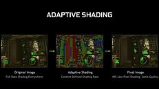
As we've seen with NVIDIA's Turing implementation for Variable Rate Shading, this performance-enhancing technique works in two ways: motion adaptive shading and content adaptive shading. Motion adaptive shading basically takes input from previous frames in order to calculate which pixels are moving fast across the screen, such as with a racing perspective - fast-flying detail doesn't stay focused in our vision so much that we can discern a relative loss in shading detail, whilst stationary objects, such as the focused hypercar you're driving, are rendered in all their glory. Valuable compute time can be gained by rendering a coarse approximation of the pixels that should be in that place, and upscaling them as needed according to the relative speed they are moving across the frame. Content adaptive shading, on the other hand, analyzes detail across a scene, and by reducing shading work to be done across colors and detail that hasn't had much movement in the previous frame and frames - saves frame time.

Microsoft's xCloud is a Push Towards Game Streaming Future, Powered by AMD

Microsoft has announced their xCloud initiative, a game streaming effort that looks to bridge the gap between local and stream-based gaming. xCloud is looking to bring true, platform-agnostic gaming with much lower bandwidth requirements due to a number of technologies being researched and worked on by Microsoft. Chief among these are low-latency networking, encoding, and decoding advances - all crucial parts of the puzzle for solving latency and poor image quality issues. xCloud aims to allow for "high-quality experiences at the lowest possible bitrates that work across the widest possible networks" - with 4G and 5G support. For now, the test version of xCloud only requires a minimum 10 Mbps connection, which is already very impressive in abstract - though of course it would require more info on the rendering specs being delivered to the recipient's system for deeper analysis.

One big takeaway here is that this xCloud initiative is fully powered by AMD's own hardware - as it should be. Using AMD custom hardware such as that found within Microsoft's Xbox consoles takes away the work and investment in building even more emulation capabilities on a server level, which would only add additional overhead to the streaming service. By using AMD's own custom hardware, Microsoft circumvents this issue - but entrenches itself even more on AMD's own product portfolio, both now and in the foreseeable future.

Return to Keyword Browsing
Apr 29th, 2024 17:04 EDT change timezone

New Forum Posts

Popular Reviews

Controversial News Posts