News Posts matching #engineering sample

Return to Keyword Browsing

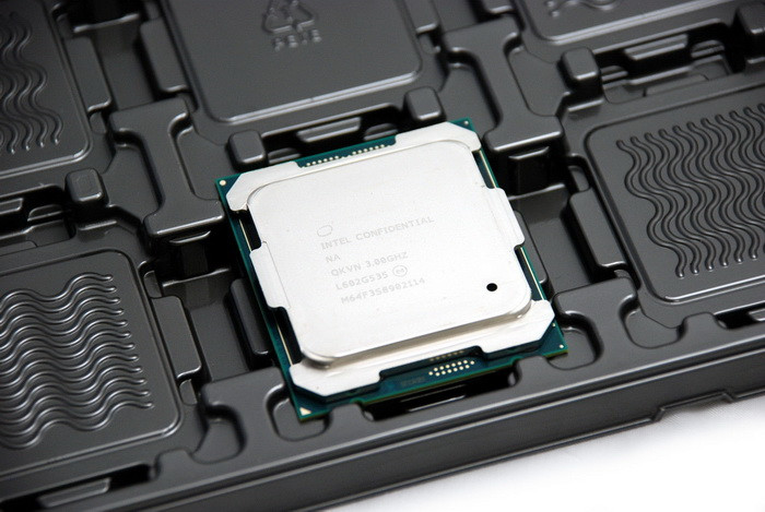
AMD "Zen" Processor Integrated Chipset Has USB 3.1 Issues, Could Escalate Costs

With its next-generation processors and APUs based on the "Zen" micro-architecture, AMD is integrating the chipset into the processor/APU die, making motherboards entirely chipset-free. This on-die chipset, however, is rumored to be facing issues with its integrated USB 3.1 controllers, according to industry sources. AMD sourced the design for the integrated USB 3.1 controllers from ASMedia. The company has a tendency of sourcing integrated controller IP from third-party manufacturers (eg: its SATA controllers and port-multipliers in the past have been sourced from Silicon Image).

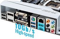
Motherboard manufacturers are noticing significant drops in USB 3.1 bandwidths with increase in circuit distances (think wiring running from the AM4 socket to USB 3.1 front-panel headers on the bottom-right corner of a motherboard). Board designers are reportedly having to use additional retimer and redriver chips to get acceptable bandwidths over such ports, and in some cases even entire USB 3.1 controllers, eating into the platform's PCIe budget and escalating costs.

Intel Core i7-6950X Engineering Sample Sells for $1950

Ahead of their launch, industry partners with engineering samples (ES) of unreleased processors make a killing on Ebay. The same was true for one lucky user of a Core i7-6950X ten-core processor ES. Listed for auction on Ebay, the chip sold for $1,950. High-resolution pictures of the chip reveal that it could ship with a core clock speed of 3.00 GHz, which is not surprising considering how low Intel has been clocking its high core-count chips to respect 140W TDP, over the past few generations. The i7-6950X is based on Intel's 14 nm "Broadwell-E" silicon, and will be compatible with existing socket LGA2011v3 (X99 chipset) motherboards, with BIOS updates, when it hits the shelves later this month. Intel's policy on engineering samples, which its partners agree to before receiving samples, states that engineering samples issued by the company, are its property.

Intel "Skylake" to be 6th Generation Core Series, First i7-6700K Benchmarks

Intel's next major CPU architecture, codenamed "Skylake," could be classified as the company's 6th generation Core processor family. It will succeed the brief stint Core "Broadwell" will have at the market, with no major chips for PC enthusiasts to look forward to. The Core i7-6700K appears to be the flagship product based on the Skylake-D silicon, succeeding the i7-4770K and i7-4790K. The Core i5-6600K will succeed the i5-4670K and i5-4690K.

The i7-6700K is a quad-core chip, with HyperThreading enabling 8 logical CPUs. Its nominal clock will be 4.00 GHz, with a rather shallow 4.20 GHz Turbo Boost frequency. It will feature an 8 MB L3 cache, and an integrated memory controller that supports both DDR4 and DDR3 memory types. This makes Skylake a transition point for the mainstream PC market to gradually upgrade to DDR4. You'll have some motherboards with DDR3 memory slots, some with DDR4 slots, and some with both kinds of slots. The resulting large uncore component, and perhaps a bigger integrated GPU, will result in quad-core Skylake parts having TDP rated as high as 95W, higher than current Haswell quad-core parts, with their 88W TDP.

Intel Haswell TSX Erratum as Grave as AMD Barcelona TLB Erratum

Intel's "Haswell" micro-architecture introduced the transactional synchronization extensions (TSX) as part of its upgraded feature-set over its predecessor. The instructions are designed to speed up certain types of multithreaded software, and although it's too new for any major software vendor to implement, some of the more eager independent software developers began experimenting with them, only to discover that TSX is buggy and can cause critical software failures.

The buggy TSX implementation on Core "Haswell" processors was discovered by a developer outside Intel, who reported it to the company, which then labeled it as an erratum (a known design flaw). Intel is addressing the situation by releasing a micro-code update to motherboard manufacturers, who will then release it as a BIOS update to customers. The update disables TSX on affected products (Core and Xeon "Haswell" retail, and "Broadwell-Y" engineering samples).

Seagate Begins Testing 8 TB Hard Drives Among Enterprise Customers

With its 6 TB desktop hard drives selling for as low as $300, Seagate is pushing up the density envelope. The company is ready with functional engineering samples of its 8 TB (8,000 GB) hard drives, and has sent them over to major enterprise (hosting / cloud) customers for reliability testing and feedback. Seagate CEO Steve Luczo revealed this, at last week's Q4FY earnings call, responding to a question.

Seagate is eyeing customers among cloud storage providers with its gargantuan hard drives. Cost-effective cloud storage is being seen as the biggest driver of storage capacity expansion among hard drive makers. On the subject of its upcoming drives, Luczo stated: "While it's still early in the development of our Kinetic object-based storage platform, we are in deep technical discussions with a very broad-base of enterprise customers. We believe our focus on developing key values for object-based storage will make the Kinetic platform a differentiated offering in the cloud storage marketplace." Seagate didn't mention when it plans to actually launch the 8 TB drive, as that would depend on the kind of feedback it receives from those customers.

NVIDIA Moving Around the Fabled GeForce GTX TITAN II

NVIDIA is moving around engineering samples of what it describes as "GM200 A1 graphics processor," in its shipping manifest. The sample was making its way from Taiwan, to Bangalore, India, from where it's likely pushed to the company's facilities in Bangalore and Hyderabad. A1 steppings of NVIDIA chips are usually pre-production, and bound for just a few more rounds of testing, before being upgraded to "A2" and mass-produced. German tech site 3DCenter.org also pulled out some likely specifications from its sources.

To begin with, the GM200, like the GM204, will be built on existing 28 nm silicon fabrication process, as both NVIDIA and AMD appear to have suffered design setbacks due to their common foundry partner, TSMC, not being able to set its next-gen 20 nm node up to speed in time. The GM200 is expected to feature over 4,000 CUDA cores, although the exact number is unknown. It is expected to widen the memory bus to 512-bit. Given the existing process, the GPU will be huge. Over 600 mm² huge. NVIDIA will probably bank on the energy efficiency of its "Maxwell" architecture to cope with thermal loads put out by a chip that big. The GM200-based "GeForce GTX TITAN II" could launch in the first half of 2015.

ADATA DDR4 OC Module Spotted on a Working Haswell-E HEDT System

ADATA's claim of being the first memory maker with DDR4 overclocking modules wouldn't fly with anyone, if they weren't using a live Haswell-E HEDT platform to show it off. The system appears to be using a prototype Intel X99 chipset micro-ATX motherboard by ASRock, and a Haswell-E engineering sample. The module comes with JEDEC SPD profile of 2133 MHz, but claims to offer tons of overclocking headroom. The system was wired to a display, and evidently, CPU-Z can't read the memory config. It can, however, read out DRAM clock and timings. The system was doing 1373 MHz (2746 MHz DDR), with timings of 14-14-14-36-CR2T.

GeForce GTX 880 ES Intercepted En Route Testing Lab, Features 8 GB Memory?

An engineering sample (ES) of the GeForce GTX 880 was intercepted on its way from a factory in China, to NVIDIA's development center in India, where it will probably undergo testing and further development. The shipping manifest of the courier ferrying NVIDIA's precious package was sniffed out by the Chinese press. NVIDIA was rather descriptive about the ES, in its shipping declaration. Buzzwords include "GM204" and "8 GB GDDR5," hinting at what could two of the most important items on its specs sheet. GM204 is a successor of GK104, and is rumored to feature 3,200 CUDA cores, among other things, including a 256-bit wide memory bus. If NVIDIA is cramming 8 GB onto the card, it must be using some very high density memory chips. The manifest also declares its market value at around 47,000 Indian Rupees. It may convert to US $780, but adding all taxes and local markups, 47,000 INR is usually where $500-ish graphics cards end up in the Indian market. The R9 290X, for example, is going for that much.

Core i7 "Haswell-E" Engineering Sample Pictured

Here's the first picture of Intel's next-generation Core i7 HEDT (high-end desktop) processor, codenamed "Haswell-E." Based on Intel's latest "Haswell" micro-architecture, the chip will be Intel's first HEDT processor to ship with eight cores, and the first client CPU to ship with next-generation DDR4 memory interface. In addition to IPC improvements over "Ivy Bridge" that come with "Haswell," the chip integrates a quad-channel DDR4 integrated memory controller, with native memory speeds of DDR4-2133 MHz; a PCI-Express gen 3.0 root complex with a total of 40 PCI-Express lanes, and yet the same DMI 2.0 (4 GB/s) chipset bus.

Built into the LGA2011-3 socket, "Haswell-E" will be incompatible with current LGA2011 motherboards, as the notches of the package will vary from LGA2011 "Ivy Bridge-E." Intel will introduce the new X99 Express chipset, featuring all 6 Gb/s SATA ports, integrated USB 3.0 controllers, and a PCI-Express gen 2.0 root complex for third-party onboard controllers. Interestingly, there's no mention of SATA-Express, which Intel's next-generation 9-series chipset for Core "Broadwell" platforms reportedly ships with; and X99 isn't looking too different from today's Z87 chipset. With engineering samples already out, it wouldn't surprise us if Intel launches "Haswell-E" along the sidelines of any of next year's big-three trade-shows (CES, CeBIT, and Computex).

G.Skill Showcases DDR4 System Memory and Live Demo of DDR3-3000 at IDF

G.SKILL International Co. Ltd., the world's leading designer and manufacturer of extreme performance memory, proudly displays several engineering sample DDR4 modules at the Intel Developer Forum (IDF). The next generation of DDR memory is still under development, and G.SKILL is working to push the new technology to its limits in the future. G.SKILL also features a live demo of DDR3 3000MHz 32GB (8x4GB) with the Intel Core i7-4960X CPU and ASUS X79-Deluxe motherboard. Driving the new Ivy Bridge-E processor to new limits, G.SKILL looks forward to offer a wide range of high performance memory kits on the Intel X79 platform.
A video presentation follows.

More Core i7-4960X "Ivy Bridge-E" Benchmarks Surface

More benchmarks of Intel's upcoming socket LGA2011 flagship client processor, the Core i7-4960X "Ivy Bridge-E," surfaced on the web. Tom's Hardware scored an engineering sample of the chip, and wasted no time in comparing it with contemporaries across three previous Intel generations, and AMD's current generation. These include chips such as the i7-3970X, i7-4770K, i7-3770K, i7-2700K, FX-8350, and A10-5800K.

In synthetic tests, the i7-4960X runs neck and neck with the i7-3970X, offering a 5 percent performance increment at best. It's significantly faster than the i7-3930K, Intel's $500-ish offering for over 7 quarters running. Its six cores and twelve SMT threads give it a definite edge over quad-core Intel parts in multi-threaded synthetic tests. In single-threaded tests, the $350 i7-4770K is highly competitive with it. The only major surprise on offering is power-draw. Despite its TDP being rated at 130W, on par with the i7-3960X, the i7-4960X "Ivy Bridge-E" offers significantly higher energy-efficiency, which can be attributed to the 22 nm process on which it's built, compared to its predecessor's 32 nm process. Find the complete preview at the source.

Intel Core i7-4960X De-Lidded

Coolaler.com community member "Toppc" scored an engineering sample of Intel's upcoming Core i7-4960X "Ivy Bridge-E" socket LGA2011 processor, and wasted no time in taking a peek inside its integrated heatspreader (IHS). Beneath the adhesive layer that holds the IHS to the package, which could be fairly easily cut through, "Toppc" discovered that Intel is using a strong epoxy/solder to fuse the processor's die to the IHS, and not a thermal paste, like on Core i7-3770K. Solders tend to have better conductivity than pastes, but make it extremely difficult to de-lid the processors, not to mention potentially disastrous. In the process of delidding this chip, "Toppc" appears to have knocked out a few components around the die. Unless you're good at precision soldering, something like that would be a fatal blow to your $1000 investment.

Intel Core i7-4770K Overclocked to 7 GHz

Launch of Intel's Core i7-4770K "Haswell" processor may be a month away, but the chip has been in circulation for some time now. An overclocker going by the handle "rtiueuiurei" managed to get an engineering sample of the chip past the 7 GHz mark, 7012.65 MHz to be precise. A base clock of 91.07 MHz, multiplier of 77.0x, and a staggering 2.56V core voltage, unless CPU-Z read it wrong. A single 2 GB memory module was used; no other details were revealed. Core i7-4770K and a fleet of compatible socket LGA1150 motherboards launch around the first week of June.

AMD Radeon HD 7990 "Malta" Listed on Ebay

A lucky bloke who managed to score an engineering sample of AMD's upcoming Radeon HD 7990 sought to make a quick buck by auctioning it on Ebay. An opening bid of $0.99, and 36 bids (ATP) later, the auction has reached the $1,125 mark. The engineering sample is said to ship with clock speeds of 950 MHz core, and 6.00 GHz memory. The dual-GPU graphics cards ships with two fully-loaded AMD "Tahiti" GPUs, with 2048 stream processors each, and a 384-bit memory interface holding 3 GB of GDDR5 memory, each. If anything the Ebay listing gave us some gorgeous pictures of the beast.

First NVIDIA GeForce Titan 780 Performance Numbers Revealed

The rumor mill is spinning to galeforce (or should we say GeForce) winds. Its newest sack of flour points at what could be the first performance figure of NVIDIA's upcoming GeForce Titan 780 flagship single-GPU graphics card. Circulating among various Chinese tech publications is this 3DMark 11 Xtreme Preset screenshot from the PCinLife community, in which a lucky bloke claimed access to a GeForce Titan 780 engineering sample, and a driver to get it to work. In the scribbled out 3DMark 11 Xtreme Preset score screenshot (below), the source claims the fabled graphics card can singlehandedly score X7107 points. For reference, a GeForce GTX 690 usually scores in the region of X6000 points, and a GTX 680 around X3300. If true, NVIDIA has something truly remarkable up its sleeves, maybe the second coming of 8800 GTX. From older reports, we know that the GeForce Titan is expected to ship sooner than most people think, some time in February.

Mass Production at Intel's 14 nanometer Node Begins This Year

In addition to the industry's first fully-patterned 450 mm wafer, Intel announced that its 14 nanometer silicon fabrication node at three of its fabs will begin this year. The next leap forward from 22 nm, on which two of the company's CPU generations "Ivy Bridge" and "Haswell" are based, the 14 nm node will eventually facilitate production of the company's 5th generation Core "Broadwell" processors, which are due to arrive in 2014. Given the pace at which the 14 nm node is being developed, some of the first Broadwell Core chips, at least engineering samples, will be released to the industry within 2013. Among the three Intel facilities with 14 nm nodes are D1X, located in Oregon; Fab 42, located in Arizona; and Fab 24, located in Ireland.

Intel, Facebook Collaborate on Future Data Center Rack Technologies

Intel Corporation announced a collaboration with Facebook to define the next generation of rack technologies used to power the world's largest data centers. As part of the collaboration, the companies also unveiled a mechanical prototype built by Quanta Computer* that includes Intel's new, innovative photonic rack architecture to show the total cost, design and reliability improvement potential of a disaggregated rack environment.

"Intel and Facebook are collaborating on a new disaggregated, rack-scale server architecture that enables independent upgrading of compute, network and storage subsystems that will define the future of mega-datacenter designs for the next decade," said Justin Rattner, Intel's chief technology officer during his keynote address at Open Computer Summit in Santa Clara, Calif. "The disaggregated rack architecture includes Intel's new photonic architecture, based on high-bandwidth, 100 Gbps Intel Silicon Photonics Technology, that enables fewer cables, increased bandwidth, farther reach and extreme power efficiency compared to today's copper based interconnects."

Intel "Bay Trail" Platform and "Valleyview" Atom SoC Detailed

Intel's next-generation Atom processor platform, codenamed "Bay Trail" doesn't arrive before 2014, but that's not enough to stop the company from talking at great lengths about it. A new presentation intended for Intel's pals in the PC industry was leaked on German tech-forum 3DCenter.org, and reveals quite a bit more about the platform than the Bay Trail-T we already know about.

The first two slides (below) detail key scoring points of the platform over its predecessor, the "Cedar Trail." These include a true single-chip SoC (with complete integration of the chipset into the processor die), being built on the 22 nm Tri-gate transistor fab process, up to four x86-64 cores with out-of-order execution capabilities, 7th generation Intel graphics that features DirectX 11 and supports resolutions as high as 2560 x 1600 pixels, a native USB 3.0 controller, and support for DDR3L memory, that allows device makers to do away with DIMM/SO-DIMM modules to conserve board foot-print, using smaller, space-optimized DRAM chips on the main PCB.

Razer Project Fiona On, Seeks FCC Approval

Earlier this month, Razer asked the gaming community to show their support for its ambitious "Project Fiona," (the development of an ergonomic, gaming-grade tablet). It looks like they have it, and are proceeding with its development. An engineering sample of the device showed up at FCC labs for approval. Only devices at a very advanced stage of development reach regulators such as the FCC and CE. The FCC document detailing "Fiona" lists the device as having a 5600 mAh battery, and a game controller accessory (the handlebar controller), which has a battery pack of its very own.

ASUS Maximus V Gene Helps Crack DDR3-3256 Dual-Channel 16 GB Memory

An anonymous overclocker cracked a staggering DRAM speed (for dual-channel), using Intel Core i7-3770K processor (engineering sample) and ASUS Maximus V Gene motherboard, at DDR3-3256 MHz. The overclocker started off at DDR3-3153 (~1576 MHz actual) on boot, and carefully notched it up to DDR3-3256 (1628 MHz actual) in Windows. 16 GB of memory of an unknown make, was used.

What makes the feat impressive is that such DRAM clock speeds are difficult for dual-channel/multiple-module setups, and reserved only for single-module feats. Ahead of the launch of the 3rd Generation Core "Ivy Bridge" platform, every motherboard vendor is covertly showing off similar overclocking feats.

A video recording of the feat follows.

More Pictures of GK104 Reference Board Surface

Here is a brief compilation of all the new images of the upcoming NVIDIA GeForce Kepler high-performance product, which our forum members posted through the day. The pictures reinforce the 3QTR picture that surfaced this Thursday, and full-length picture of the PCB that surfaced earlier this month. The first picture below, reveals what is essentially the card that was pictured yesterday, with its cooler shroud taken out. You will find a conventional air-channel cooler design. A lateral-flow fan, which looks similar to the one used in GeForce GTX 580/570), directs air through a dense aluminum channel array, which draws heat from key components such as the GPU, memory, and VRM, using a vapor-chamber plate (again, similar to the one used on high-end GeForce GTX 500 series). Towards the rear portion, you'll spot the piggy-backed 6+6-pin PCIe power connector cluster. You will also find the black rugged metal base-plate flowing along the full length of the PCB, structurally reinforcing it, and performing some cooling functions.

Moving on, the second picture reveals the same VRM area we saw earlier, on the green-colored PCB engineering sample, with its five NVVDD phases. The third picture is the first, of the reverse side of the PCB. Revealing most of the solder points, and electrical circuitry. The driver ICs of each of the NVVDD phases can be seen here. These two pictures confirm that the retail version of the GK104 product will feature a black PCB (the brown tinge is natural, due to the dense network of traces and ground layers, made of copper). The fourth picture reveals what looks like NVIDIA's Media Kit. Reputed reviewers get a NVIDIA-branded "media kit", which contains the graphics card sample to review, and other relevant documentation in printed form, along with a driver CD, and other accessories. These cards are not branded by any AIC partner, and are 100% compliant to NVIDIA's reference design and clock speeds.

Many Thanks to our community members JaredPace and CrapDaddy.

GK104 PCB Pictured in Full

Here is the first true-color picture of the GeForce Kepler 104 (GK104) reference PCB shot in full (well, almost, excluding the uneventful PCIe bus connector). The picture provides a panoramic view of the card's VRM as shown in a drawing posted earlier this day, and reveals the strange double-decker power connector. The card is loaded with a 5-phase NVVDC configuration, as detailed in an older article. It also confirms that the GK104 has a 256-bit wide memory interface, with likely 2 GB standard memory amount. This is also the first picture of the GK104 ASIC, which has square package, and somewhat square die. While the PCB is green in color, it's most likely an engineering sample. The final product (branded GeForce GTX 680 / GTX 670 Ti), could have a black-colored one.

10-core Ivy Bridge-EP Sample Tested

The Ivy Bridge LGA1155 processors inbound for April are mom and pop PC chips in front of the monstrosities Intel has planned for the enterprise (and possibly high-end desktop/HEDT) markets, based on the architecture. An 10-core Ivy Bridge-EP engineering sample, made it to the right hands in Taiwan (wrong hands for Intel), that wasted no time in putting them through some tests.

The 10-core Ivy Bridge-EP/EX chip (LGA2011, 2P-capable) features 10 next-generation cores clocked at 2.80 GHz, with 256 KB L2 cache per core, 30 MB shared L3 cache, and HyperThreading technology that enables 20 logical CPUs. This chip crunched WPrime 1024M in 158.5 seconds, and scores 41.78X relative speed in Fritz chess when just 8 of its 20 threads are put to use. You can also find some pretty screen shots of CPU-Z with its long processor selection list and Windows 8 task manager.

Dishonest Intel OEM Engineers To Get Five Years Behind Bars

The Taiwan Criminal Investigation Bureau has been doing a bit of investigating and has arrested four engineers working for Intel's OEM partners (names not disclosed) for flogging Engineering Sample (ES) processors on eBay. ES processors are intended strictly for qualification testing purposes for development of new products by OEM's and are only loaned to them under strict non-disclosure agreements, hence putting these on eBay is illegal. The Bureau searched the suspects houses last month and found 178 ES CPU's, worth around $800,000. Note that this value seems to be somewhat high, as it would make each CPU worth around $4,500. We will update this article if new values come to light. Also, this is not a new operation that has been busted, since the suspects had admitted to selling around 500 ES CPU's since 2009. For their efforts, the fab four now face five years in prison.

It should be noted for anyone contemplating the purchase of such dodgy CPU's on eBay or similar places, that they may be overstressed and contain faults, due to the intensive and sometimes destructive testing they go through.
Return to Keyword Browsing
May 1st, 2024 20:40 EDT change timezone

New Forum Posts

Popular Reviews

Controversial News Posts