News Posts matching #GM204

Return to Keyword Browsing

NVIDIA GeForce "Ada Lovelace" Memory Bus-width Info Leaked

The deluge of NVIDIA leaks continue following the major cyber-attack on the company, with hackers getting away with sensitive information about current and upcoming products. The latest in this series covers the memory bus widths of the next-generation RTX 40-series GPUs based on the "Ada Lovelace" graphics architecture. There is early-information covering the streaming multiprocessor (SM) counts of each GPU, and their large on-die caches.

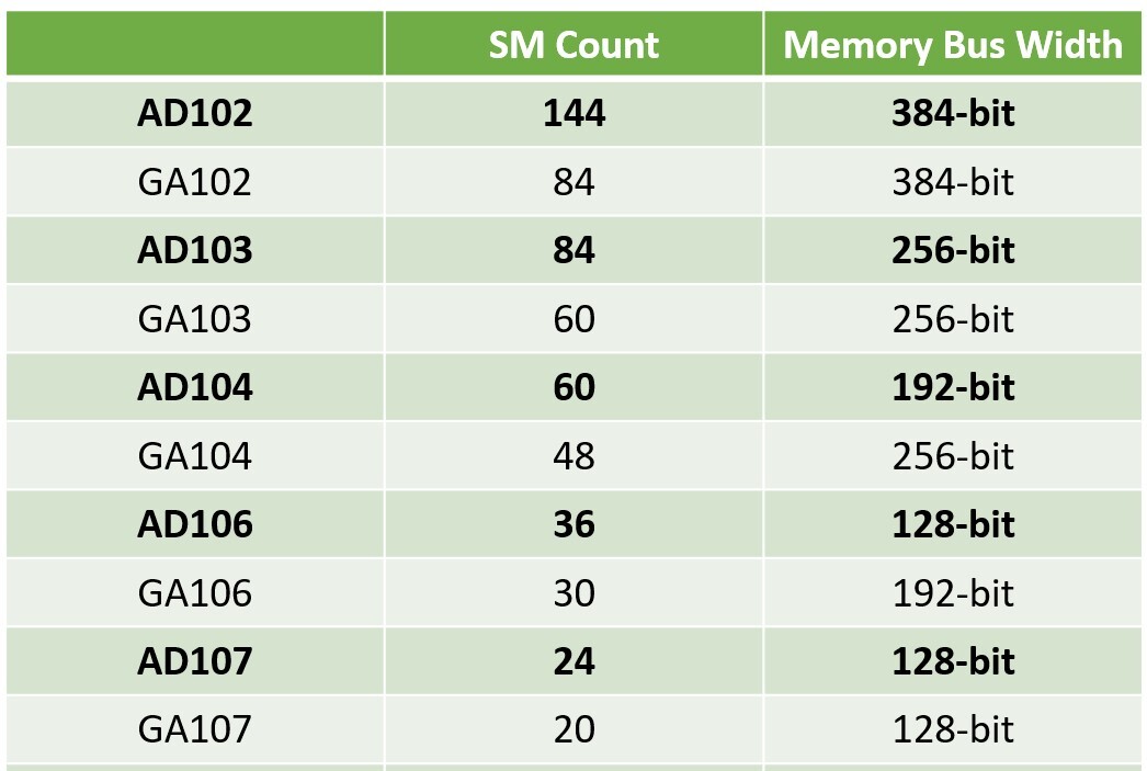
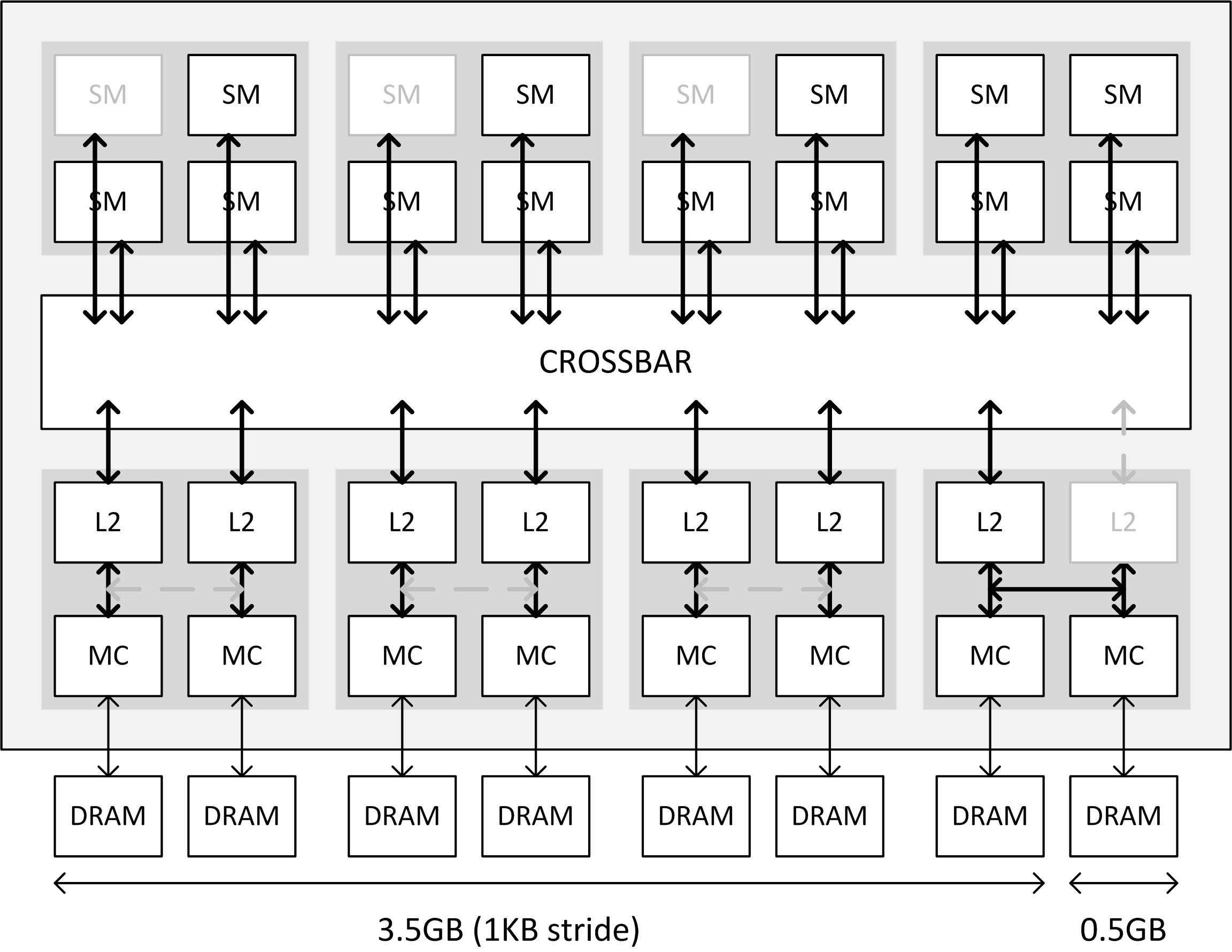
The top-of-the-line AD102 silicon allegedly has a 384-bit wide memory bus, similar to its predecessor. The next-best AD103 silicon has a 256-bit wide memory bus. Things get very interesting with the AD104, which has a 192-bit wide memory bus. The AD104 is a revelation here, because it succeeds a long line of NVIDIA GPUs with 256-bit memory buses (eg: GA104, TU104, GP104, GM204, etc). This confirms the theory that much like AMD, NVIDIA is narrowing the memory bus widths in the lower segments to cut board costs, and compensate for the narrower bus-width with large on-die caches, high memory data-rates, and other memory-management optimizations.

NVIDIA Reportedly Stops Production of Certain "Maxwell" GPUs

Paving the way for its next-generation "Pascal" architecture-based performance-thru-enthusiast GPUs, NVIDIA reportedly halted further production of certain current-generation "Maxwell" GPUs. HWBattle reports that production of the GM204-based GeForce GTX 980, the popular GTX 970, and GM200-based GTX 980 Ti have seen production halts, to let the market digest existing inventories of the three cards; and letting NVIDIA's add-in card (AIC) partners prepare to stock up next-generation graphics cards, beginning with at least three SKUs based on the GP104 silicon, in June 2016.

NVIDIA Readies Three GP104 "Pascal" Based SKUs for June 2016

NVIDIA is reportedly giving final touches to no less than three SKUs based on the 16 nm GP104 silicon, to launch some time this June. The ASIC markings for the chips that drive these SKUs are "GP104-400-A1," "GP104-200-A1" and "GP104-150-A1." If you recall, NVIDIA last reserved the "-400-A1" markings for the GeForce GTX 980 (GM204-400-A1), and the "-200-A1" for the GTX 970 (GM204-200-A1).

The GP104-150-A1 is a mystery ASIC. Either it will drive a more affordable third desktop SKU based on the GP104, or could signify a mobile SKU. The company plans to launch the products based on the GP104-400-A1 and GP104-200-A1, logical successors to the GeForce GTX 980 and GTX 970, in early June. The GP104-150-A1, on the other hand, could see the light of the day in mid-June.

Eurocom Announces Sky X9E VR-Ready Gaming Notebook

Eurocom is launching the Sky X9E Extreme Edition unlocked, high performance "desktop Laptop" with Intel Core i7-6700K, NVIDIA GeForce GTX 980, 64 GB DDR4 memory and a beautiful 4K 17.3" display. Eurocom customers now have an ultra-high performance, fully upgradeable mobile platform that they have utmost freedom to control and to push it to the limits.

Equipped with the most powerful components ever assembled in a laptop form factor and now with the unlocked capability to push the performance to otherworldly levels. Eurocom provides an unlocked BIOS along with an Overclocking Seminar with overclocking expert Mr. Fox so users have a quick rundown on how to best push their new EUROCOM Sky X9E to the limits as well as setting limitations and safe guards for safe operation.

NVIDIA Releases Full-featured GeForce GTX 980 for Notebooks

NVIDIA released a reference board for a full-featured GeForce GTX 980 GPU for the notebook platform. This is different from the GeForce GTX 980M launched last October, which features just 1,536 of the 2,048 CUDA cores physically present on the GM204 silicon. The new GTX 980 for notebooks is targeted at large desktop-replacement gaming notebooks, and features all components present on the silicon.

The GeForce GTX 980 for Notebooks reference board features 4-8 GB of GDDR5 memory across the chip's 256-bit wide memory bus, a 4-8 phase VRM, and clock speeds which are close to the desktop reference board. The GPU is clocked around 1175 MHz, and the memory ticks at 7.00 GHz (GDDR5-effective). It's primed for overclocking beyond 1400 MHz core, and 7.50 GHz memory. It also offers fan-control for users, that adjusts clock speeds according to the fan-curve. Various gaming notebook makers are announcing variants of their premium notebooks featuring this board.

NVIDIA Tapes Out "Pascal" Based GP100 Silicon

Sources tell 3DCenter.org that NVIDIA has successfully taped out its next big silicon based on its upcoming "Pascal" GPU architecture, codenamed GP100. A successor to GM200, this chip will be the precursor to several others based on this architecture. A tape-out means that the company has successfully made a tiny quantity of working prototypes for internal testing and further development. It's usually seen as a major milestone in a product development cycle.

With "Pascal," NVIDIA will pole-vault HBM1, which is making its debut with AMD's "Fiji" silicon; and jump straight to HBM2, which will allow SKU designers to cram up to 32 GB of video memory. 3DCenter.org speculates that GP100 could feature anywhere between 4,500 to 6,000 CUDA cores. The chip will be built on TSMC's upcoming 16 nanometer silicon fab process, which will finally hit the road by 2016. The GP100, and its companion performance-segment silicon, the GP104 (successor to GM204), are expected to launch between Q2 and Q3, 2016.

GALAX Launches Liquid-Cooled HOF GTX 970 and GTX 980 Graphics Cards

GALAX, a leading manufacturer and innovator of extreme performance gaming hardware, today announced the long awaited custom water-cooled HOF series. Pushing the limits is the Hall of Fame series' reason for being-fueling the passion for World record breaking overclocks and peerless in-game performance. This passion is rivaled only by GALAX's dedication to engineering the most capable, powerful and uncompromised hardware for the task, and the results have earned HOF series graphics cards a reputation as the best since their global debut in 2013.

Working in-conjunction with Diamond Cooling based in Europe, specialists in all things custom and cool, GALAX has developed a water cooling solution designed to fully unleash the raw potential of the GTX 980 and 970 HOF graphics cards with the unprecedented cooling capacity needed for extreme overclocks.

NVIDIA GeForce GTX TITAN-X Specs Revealed

NVIDIA's GeForce GTX TITAN-X, unveiled last week at GDC 2015, is shaping up to be a beast, on paper. According to an architecture block-diagram of the GM200 silicon leaked to the web, the GTX TITAN-X appears to be maxing out all available components on the 28 nm GM200 silicon, on which it is based. While maintaining the same essential component hierarchy as the GM204, the GM200 (and the GTX TITAN-X) features six graphics processing clusters, holding a total of 3,072 CUDA cores, based on the "Maxwell" architecture.

With "Maxwell" GPUs, TMU count is derived as CUDA core count / 16, giving us a count of 192 TMUs. Other specs include 96 ROPs, and a 384-bit wide GDDR5 memory interface, holding 12 GB of memory, using 24x 4 Gb memory chips. The core is reportedly clocked at 1002 MHz, with a GPU Boost frequency of 1089 MHz. The memory is clocked at 7012 MHz (GDDR5-effective), yielding a memory bandwidth of 336 GB/s. NVIDIA will use a lossless texture-compression technology to improve bandwidth utilization. The chip's TDP is rated at 250W. The card draws power from a combination of 6-pin and 8-pin PCIe power connectors, display outputs include three DisplayPort 1.2, one HDMI 2.0, and one dual-link DVI.

GTX 970 Memory Drama: Plot Thickens, NVIDIA has to Revise Specs

It looks like NVIDIA's first response to the GeForce GTX 970 memory allocation controversy clearly came from engineers who were pulled out of their weekend plans, and hence was too ambiguously technical (even for us). It's only on Monday that NVIDIA PR swung into action, offering a more user-friendly explanation on what the GTX 970 issue is, and how exactly did they carve the GM204 up, when creating the card.

According to an Anandtech report, which cites that easy explanation from NVIDIA, the company was not truthful about specs of GTX 970, at launch. For example, the non-public document NVIDIA gave out to reviewers (which gives them detailed tech-specs), had clearly mentioned ROP count of the GTX 970 to be 64. Reviewers used that count in their reviews. TechPowerUp GPU-Z shows ROP count as reported by the driver, but it has no way of telling just how many of those "enabled" ROPs are "active." The media reviewing the card were hence led to believe that the GTX 970 was carved out by simply disabling three out of sixteen streaming multiprocessors (SMMs), the basic indivisible subunits of the GM204 chip, with no mention of other components like the ROP count, and L2 cache amount being changed from the GTX 980 (a full-fledged implementation of this silicon).

Aorus X5 Gaming Notebook Offers Ultra HD in a 15.6-inch Package

Aorus X5 is the company's latest gaming notebook, featuring one of the industry's sharpest displays, based on the IGZO technology. This 15.6-incher offers Ultra HD (3840 x 2160 pixels) display resolution. Driving the display is an NVIDIA GeForce GTX 965M SLI setup, with 4 GB of GDDR5 memory per GPU. Based on the GM204 silicon, the GTX 965M features 1024 CUDA cores running at 945 MHz, and a 128-bit wide GDDR5 memory bus, running at 5.00 GHz. Our educated guess is that GTX 965M SLI should offer performance comparable to a single, overclocked GTX 980, if not more. By Aorus' own benchmarks, this notebook yields P12000 in 3DMark 11. Other chops of the Aorus X5 include a Core i7 CPU, up to 32 GB of dual-channel memory, M.2 SSD storage, 2.29 cm thickness with the lid closed, and just under 2.5 kg of weight.

Possible NVIDIA GM200 Specs Surface

Somebody sent our GPU-Z validation database a curious looking entry. Labeled "NVIDIA Quadro M6000" (not to be confused with AMD FirePro M6000), with a device ID of 10DE - 17F0, this card is running on existing Forceware 347.09 drivers, and features a BIOS string that's unlike anything we've seen. Could this be the fabled GM200/GM210 silicon?

The specs certainly look plausible - 3,072 CUDA cores, 50 percent more than those on the GM204; a staggering 96 ROPs, and a 384-bit wide GDDR5 memory interface, holding 12 GB of memory. The memory is clocked at 6.60 GHz (GDDR5-effective), belting out 317 GB/s of bandwidth. The usable bandwidth is higher than that, due to NVIDIA's new lossless texture compression algorithms. The core is running at gigahertz-scraping 988 MHz. The process node and die-size are values we manually program GPU-Z to show, since they're not things the drivers report (to GPU-Z). NVIDIA is planning to hold a presser on the 8th of January, along the sidelines of the 2015 International CES. We're expecting a big announcement (pun intended).

NVIDIA Breathes Life into Kepler with the GK210 Silicon

NVIDIA's "Maxwell" architecture may have got a rather low-key debut with the GeForce GTX 750 Ti, but nobody saw its performance-segment derivative, the GM204 silicon, driving the GeForce GTX 980 and the GTX 970. The new architecture makes its predecessor, the "Kepler" look inefficient in comparison. It looks like NVIDIA still thinks Kepler is competitive to competition from AMD (GCN) and Intel (Knights Corner), in the high-performance computing era.

The problems here are NVIDIA already launched a GK110 based Tesla HPC card, and its big "Maxwell" chip is nowhere in sight. The GM204 has limited memory bandwidth, and its texture-compression mojo can't bail out bandwidth-hogging HPC applications. The solution? Develop a new big silicon based on "Kepler." Enter, the GK210. That's right, the G-K-210. Launched today with the Tesla K80 dual-chip HPC accelerator, this chip could feature design improvements over the GK110, while offering memory bandwidth and sizes not possible on the GM204.

EK Introduces Short Type GeForce GTX 970 Water Block

EK Water Blocks, Ljubljana based premium computer liquid cooling gear manufacturer, is proud to introduce a new Full-Cover water block for reference design NVIDIA GeForce GTX 970 series graphics cards, powered by the GM204-200 Maxwell generation GPU.

EK-FC970 GTX is a high-performance Full-Cover water block which directly cools the GPU, RAM as well as VRM (voltage regulation module) as water flows directly over these critical areas thus allowing the graphics card and it's VRM to remain stable under high overclocks.

NVIDIA GeForce GTX 960 to Retain Memory Bus from GTX 970

Among other things like CUDA core and TMU counts, NVIDIA was expected to give its next mid-range graphics card, the GeForce GTX 960, a narrower memory bus, with 3 GB of memory, if not less. A sample sniffed out by India's overly transparent customs department, en route testing facilities in the country, reveal that it's not the case.

The GeForce GTX 960, according to description given in the shipping manifest of the sample, features 4 GB of memory, with a full 256-bit wide memory interface. It also reveals clock speeds to be in the neighborhood of 993 MHz core, with 6.00 GHz memory (GDDR5-effective). It doesn't, however, confirm that the GTX 960 is based on a cut-down GM204 silicon. This could still be different chip, the so-called GM206, which succeeds the GK106.

ELSA Launches GeForce GTX 980 SAC Graphics Card

ELSA launched its first custom-design GeForce GTX 980 graphics card, bearing its SAC (silent air-cooling) badge. The card retains its signature Inno3D-sourced look, featuring a cooling solution that lets you easily clean it, to keep its cooling performance up to the mark. The cooling solution consists of an aluminium fin-stack heatsink, to which heat drawn from the GPU, is fed by a number of copper heat pipes, and ventillated by a pair of fans. The shroud on which the two are suspended, can be detached, by pulling out thumb-screws. The PCB under this cooler appears to stick to NVIDIA reference design.

The GTX 980 SAC from ELSA is factory-overclock, although the overclock is nothing to write home about. The core is clocked at 1152 MHz, with 1253 MHz GPU Boost, and 7.00 GHz memory, compared to NVIDIA reference clocks of 1126 MHz core, and 1216 MHz GPU Boost. Based on the 28 nm GM204 silicon, the GeForce GTX 980 features 2,048 CUDA cores, 128 TMUs, 64 ROPs, and a 256-bit wide GDDR5 memory interface, holding 4 GB of memory. The card draws power from a pair of 6-pin PCIe power connectors. Display outputs include three DisplayPorts, and one each of HDMI 2.0 and dual-link DVI.

NVIDIA Could Review GTX TITAN-Z Pricing for the Retail Channel

Under pressure from its own recently launched GeForce GTX 980 cannibalizing its $3,000 flagship GeForce GTX TITAN-Z (you can buy GTX 980 Quad-SLI at $2,200), NVIDIA could finally review its pricing, in the retail channel. The company recently reduced its price for the OEM channel, letting pre-built gaming PC manufacturers source the card at a lower price, whether those price-savings were transferred to the end-users, is a different question. To what measure NVIDIA could lower prices of the GTX TITAN-Z, is not known at this point. Retailers like OCUK were seen offering their GTX TITAN-Z cards at a slightly reduced price, last week. Across the big pond, American retailer Newegg sold-out an ASUS-branded GTX TITAN-Z for as low as US $1,500.

In the wake of GTX 980, AMD cut prices of its dual-GPU flagship product, the Radeon R9 295X2, down to $999. It's hard to imagine that competition from this card, and the GTX 980, are the only factors driving down prices of the GTX TITAN-Z in such a big way. Could NVIDIA be working on its next dual-GPU flagship graphics card already? Perhaps one based on a pair of GM204 chips, with thermal and power requirements as low as those of the GTX 690? Watch this space for more.

Gigabyte Outs Second GeForce GTX 970 WindForce OC Graphics Card

Gigabyte rolled out its second factory-overclocked GeForce GTX 970 graphics card after the GTX 970 G1.Gaming, the GTX 970 WindForce OC (model: GV-N970WF3OC-4GD). Its board design is identical to that of the GTX 970 G1.Gaming, but its factory-overclock is milder. The card ships with factory-overclocked speeds of 1114 MHz core, 1253 MHz GPU Boost, and 7.00 GHz memory, compared to the 1178 MHz core and 1253 MHz GPU Boost of the G1.Gaming, and NVIDIA reference speeds of 1050 MHz core, and 1178 MHz GPU Boost. The card features Gigabyte's new generation WindForce 3X cooling solution, which is capable of handling heavy thermal loads, which may look surplus to requirements for a 170W GPU, but serves to keep temperatures off the hair-trigger 80°C thermal limit. Based on the 28 nm GM204 silicon, the GeForce GTX 970 features 1664 CUDA cores, 104 TMUs, 64 ROPs, and a 256-bit wide GDDR5 memory interface, holding 4 GB of memory. Expect this card to be priced around US $350.

MSI Holding Off on GTX 980 Lightning, in Anticipation of Bigger Chip

MSI is reportedly holding off on launching an overclocking-grade GeForce GTX 980 graphics card that you can ride into record-setting competitions, based on its coveted OC Series Lightning brand. The company probably wants to avoid a repeat of last year, when launch of its GeForce GTX 780 Lightning graphics card was closely trailed by NVIDIA's launch of the inherently faster GeForce GTX 780 Ti, and resulting price-cuts for the GTX 780, throwing MSI's inventories in jeopardy. The year before that, MSI launched the Radeon HD 7970 Lightning just weeks before AMD launched the faster HD 7970 GHz Edition.

MSI could stick to selling its Gaming Series GTX 980, equipped with the new Twin Frozr V cooling solution, even offering factory-overclocked variants of the card. This also leads one to wonder if NVIDIA has a third, high-end graphics card based on the GM204 silicon, on the 'cards,' one with higher clock speeds, or a higher temperature-based clock speed throttle, which is currently at a hair-trigger 80°C on the GTX 980.

EK Unveils Its NVIDIA GeForce GTX 980 Water Blocks

EK Water Blocks, Ljubljana based premium water cooling gear manufacturer, is proud to introduce full-cover water cooling solution for NVIDIA reference (NVA-1G401) design GeForce GTX 980 series graphics cards, based on Maxwell GM204 graphics processor.

EK-FC980 GTX directly cools the GPU, RAM as well as VRM (voltage regulation module) as water flows directly over these critical areas thus allowing the graphics card and it's VRM to remain stable under high overclocks.

NVIDIA Announces the GeForce GTX 980 and GeForce GTX 970

At the Game24 event held at several locations around the world, and online, NVIDIA launched its next-generation GeForce GTX 900 series high-end graphics cards, led by the GeForce GTX 980, and the GeForce GTX 970. The two are based on the company's new 28 nm GM204 silicon, derived from the "Maxwell" GPU architecture. The GeForce GTX 980 leads the pack, featuring 2,048 CUDA cores, 128 TMUs, 64 ROPs, and a 256-bit wide GDDR5 memory interface, holding 4 GB of memory.

The GeForce GTX 970, on the other hand, features 1,664 CUDA cores, 104 TMUs, 64 ROPs, and the same memory configuration. Both cards feature TDP rating of under 170W, and clock speeds above the 1 GHz mark. The GTX 980 features clock speeds of 1126 MHz core, 1216 MHz GPU Boost, and 7.00 GHz memory. The GTX 970, on the other hand, offers 1050 MHz core, 1178 MHz GPU Boost, and 7.00 GHz memory. Both cards offer 224 GB/s of memory bandwidth, but feature technologies that help them make the most of it, such as 3rd generation Delta-color compression, a lossless texture compression algorithm. The GeForce GTX 980 starts at US $549, while the GTX 970 starts at $329.

Gainward Readies GeForce GTX 970 Phantom, GTX 980 Reference

Gainward will launch three graphics cards based on the GM204 silicon later this week, its GeForce GTX 980 board, which sticks to NVIDIA's reference board design, a slightly non-reference GTX 970 which comes with reference clock speeds, and a completely non-reference Phantom Edition board, featuring the company's iconic air-pulling concealed fans, which could ship with a factory-overclock. The GTX 970 Phantom could ship with some of the highest factory-overclocks in the lineup, with core clock speeds of 1152 MHz, GPU Boost speeds of 1304 MHz, and an untouched 7.00 GHz memory.

Even More GeForce GTX 980 and GM204 Specs Tumble Out

Ahead of its launch later this week, even more details of NVIDIA's upcoming GeForce GTX 980, and the 28 nm "GM204" silicon it's based on, tumbled out. To begin with, the GM204 silicon is confirmed to be built on the 28 nm silicon fab process. The chip bigger than that of the GK104, with a die area of 398 mm², yet smaller than the GK110, which measures 581 mm². Its transistor count is 5.2 billion, about 2 billion more than the GK104.

The component hierarchy of GM204 is similar to that of the GM107 silicon, on which the GTX 750 Ti is based. The GPU features a 256-bit wide GDDR5 memory interface, and PCI-Express 3.0 x16 bus. The GigaThread Engine dispatches workload between four graphics processing clusters (GPCs), the basic subunit. Each GPC has a common raster engine shared between four streaming multiprocessors Maxwell (SMMs), which each hold 128 CUDA cores. The total CUDA core count is hence 2,048. The L2 cache has been quadrupled over GK104. The chip features 2 MB of it, compared to 512 KB on its predecessor. The GM204 features 64 ROPs, double that of the GK104, and should hence come with a strong geometry processing muscle. The chip features a revolutionary new 3-bit delta color compression technology that makes the most of the limited memory bus width of this chip.

NVIDIA GeForce GTX 980 and GTX 970 Pricing Revealed

Apparently, NVIDIA is convinced that it has a pair of winners on its hands, with its upcoming GeForce GTX 980 and GTX 970 graphics cards, and is preparing to price them steeply. The GeForce GTX 980 is expected to start at US $599, nearly the same price as the GeForce GTX 780 Ti. The GTX 970, on the other hand, will start at US $399, danger-close to cannibalizing the GTX 780.

Across the brands, the GTX 980 is launching at the same pricing AMD's Radeon R9 290X launched at; and the GTX 970 at that of the R9 290. AMD's cards have since settled down to $449 for the R9 290X, and R9 290 at $350. Both the GTX 980 and GTX 970, will be available in non-reference board designs, although reference-design GTX 980 will dominate day-one reviews. Based on the 28 nm GM204 silicon, the GTX 980 features 2,048 CUDA cores, 128 TMUs, 32 ROPs; while the GTX 970 features 1,664 CUDA cores, and 104 TMUs. Both feature 256-bit wide memory interfaces, holding 4 GB of GDDR5 memory.

NVIDIA GeForce GTX 980 Specifications Detailed Some More

NVIDIA's next-generation flagship single-GPU graphics card, the GeForce GTX 980, will feature 2,048 CUDA cores, and not the previously thought of 1,920. These 2,048 will be spread across 16 Streaming Multiprocessor Maxwell (SMM) units. Its sibling, the GeForce GTX 970, in comparison, features 1,664 cores spread across 13 SMMs. The TDP of GTX 980 is rated at just around 175W, and that of the GTX 970 at 145W. In comparison, the GK104 silicon, on the GeForce GTX 770, is rated at 230W. The kicker? Both GM204 and GK104 are based on the same 28 nm silicon fab node. Both cards feature power inputs consisting of two 6-pin PCIe power connectors. NVIDIA is expected to launch the two, on the 19th of September, 2014.

NVIDIA Readies GeForce GTX 960

It looks like GeForce GTX 980 and GTX 970 won't be the only Maxwell-based graphics cards NVIDIA plans to launch within the next 30 days. The company is readying a third SKU based on the chip, the GeForce GTX 960. The company's next sub-$300 graphics card, the GTX 960 will be launched some time in mid to late-October, 2014. The company's GTX 970 and GTX 980 will come out later this week (19th September), timed with the Game24 event. There's no word on the exact specs of the GTX 960.
Return to Keyword Browsing
Apr 26th, 2024 16:13 EDT change timezone

New Forum Posts

Popular Reviews

Controversial News Posts