 89
89
AMD FX-8150 3.60 GHz with Windows Patches Review
(89 Comments) »Introduction

First of all, I would like to thank AMD for providing the review kit (CPU, Asus motherboard and liquid cooling) G.Skill for providing a RipjawsX DDR3 memory kit, and Links for their continuous support.
The very codename for this architecture, Bulldozer, pretentious in its every way, indicated something big is coming from AMD. Something with overwhelming power, bulldozing its way to the top of the chain. The first processor architecture developed from ground up, after the Kx series, starting with K7 back in the 1999, to not so distant past and the latest successor, K10.5 and Thuban hexa core processor. In original plans, the first processor based on Bulldozer architecture was due to come out by the end of 2009, but numerous delays in development set the plan back by a year, to end of 2010. And we all know how that went, we were just introduced with upcoming Istanbul and its desktop derivate Thuban hexa core processors, still based on the same K10.5 architecture used with Deneb cores. If it were to come out a year ago, it would have made a noticeable impact, and maybe it would have justified its architecture codename – Bulldozer.
But AMD missed its train, again, and Bulldozer is thrown into the market, in a very undesirable time frame, between Intel's latest LGA1155 platform and Sandy Bridge processors, up until now a very dominating and widespread platform among all group of users, and on the other side, a Sandy Bridge-E heavy duty performance platform which will even in its weakest SKU outperform AMD's top offering. I'm sure many, if not all of you already read some of reviews of AMD's FX-8150 processor and are aware of the disappointment it left with reviewers and general public.
There's a double edge situation in late reviewing the product, after reading everyone else's work, and opinions. On one side, it's harder to approach the product reviewed with objective state of mind, and on the other hand, there's a certain motivation to find something everyone else missed, or at least round up all of the testing methods and aspects on one table, and come to an undeniable conclusion. But before we go and bench the hell out of the fastest FX comebacker we have to go through the architecture so we can get a better grasp of the performance numbers later on and what they mean.
Packaging and Contents

A standard review set was delivered by AMD for review, consisting of ASUS Crosshair V Formula motherboard (AMD 990FX chipset), AMD FX-8150 processor in retail packaging and as a separate part an AMD liquid cooler solution was delivered for better overclocking experience.
The FX-8150 retail package includes a short installation manual, FX-8150 case-badge, AMD-certified aluminum heatsink with optional liquid cooler package also available, and of course the processor itself. AMD offers a 3-year warranty for all retail processors, including this one.
AM3+ platform
After a long and somewhat successful period of AM2 and AM2+, followed by not so long ago introduced AM3 socket, for the next few years AMD is going to lean on its newest AM3+ socket platform combined with processors based on the Bulldozer architecture. The new AM3+ socket has 942 pin count, compared to 941 found on previous AM3 socket. We wont be seeing any DDR2 motherboards anymore, as the new Bulldozer processors only has a native DDR3 memory controller, but we'll get to that in more detail later on.Compatibility wise, AM3+ has kept backward compatibility with AM3 processors, but new AM3+ processors will not be supported on older AM3 platforms. In other words, you can buy an AM3+ motherboard and continue using your current AM3 Phenom II or Athlon II processor with DDR3 memory, but you can't buy an AM3+ processor and put it in your older AM3 motherboards.
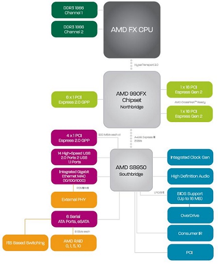
AMD's recently introduced 9-series chipset will be the heart of new AM3+ platform, but other than the name there are very few differences to older 800 series chipsets. The 900 series' flagship is an 990FX northbridge that has just two differences from its predecessor 890FX. When paired with Bulldozer, Hyper Transport will run at HT v3.1, which in theory runs up to 3200 MHz compared to HT v3.0 which runs up to 2600 MHz. This increases the bandwidth in communication between processor and the rest of the system, but it will run at HT 3.1 only with Bulldozer processors. Phenom II and Athlon II processors will run at HT 3.0 when used in any AM3+ motherboard. The Northbridge is providing in total 42 PCIe 2.0 lanes, of which 32 are for graphics cards and now support both AMD Crossfire and NVIDIA SLI; six PCIe lanes are available in 6x 1 PCIe combination, and last four PCIe lanes are reserved for A-Link Express III connection with the new SB950 Southbridge, which again, has the same specifications as the older SB850 - still no native USB 3.0 support, so AMD will have to rely on third party chips for providing USB 3.0.

To make matters more complicated, there have been AM3 boards on the market for quite some time now, using 800 series chipset and claiming to have AM3+ processor support. That is true only if those boards have implemented an AM3+ socket layout, also known as "black colored" socket featuring 942 pin holes. They will run your Bulldozer processors with proper BIOS update, but without the use of HT 3.1 support. Older AM3 boards using "white" 941 pin sockets so far offer limited support via beta BIOS updates, so please inform yourself about your motherboard CPU support before choosing to upgrade with Bulldozer sample.
Bulldozer
As stated in the introduction, Bulldozer is the name of the new architecture AMD will base future processors on, and in many ways it will lay the new foundation for AMD's core business. It will become basis for further architecture developments, something similar to K8 architecture long ago, and those foundations led to today's Phenom II processors, and K10.5 architecture revision. Although Bulldozer's architecture already had its bundle of bad critics, let's try to keep an open mind and try to understand AMD's newest product as best as we can.AMD launched the Bulldozer architecture with few keynotes, telling us what to expect from future products. In short, those keynotes were: great gaming experience, eight core processor with unlocked overclocking capabilities that would be part of a balanced performance PC, and of course new architecture. We're going to dig into that architecture, but on a small side-note, notice how they used the term "part of a BALANCED performance PC", even when launching the flagship model, that in fact should be something like "part of ULTIMATE performance PC"?

Bulldozer's architecture is based on building blocks, highly modular and adaptive designed, easily scaled to fit all demands. Its basic building block is a module, consisting of two integer cores, sharing some of the core's traditional resources; instruction fetcher and decoder, floating point unit and L2 cache memory. This makes a single Bulldozer module, in essence CMP (chip-level multiprocessing) style dual core processor. Although many would argue this is not a true dual core processor because of shared resources, unlike Intel that's using SMT (simultaneous multithreading), where two threads are processed virtually at the same time on one core, Bulldozer runs two threads trough two separate physical cores.
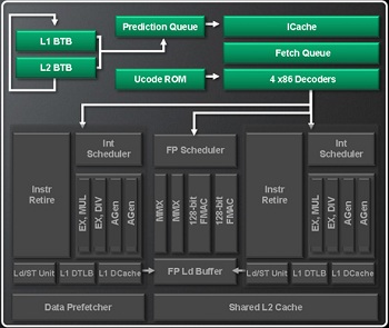
The entire process starts at newly designed front end with new prediction pipeline which tries to predict the next two instructions that are going to be used. The fetch unit loads those instructions onto four x86 decoders, one more than K10.5 had. Now we stumble upon the first possible problem in Bulldozer performance. Since the entire module front end is shared between cores, including fetch unit, it means the L1 cache is also shared between cores inside one Bulldozer module. Each module has a total of 96 KB L1 cache memory, of which 64 KB is shared two-way set associative instruction L1 cache, and each core receives 16 KB of dedicated L1 data cache memory, four-way associative. If we look at the Phenom II processor, they had 64 KB L1 data and 64 KB L1 instruction cache memory. So even with a core architecture so much more complex, L1 cache received a noticeable cut down in size.

After the decoder is done converting x86 instructions to much simpler micro-instructions, they are assigned to either floating point unit or one of the two integer units - or cores if you like the sound of it. Another thing that's shared here, a single floating point unit per module, heavily upgraded compared to Phenom II processors. Now featuring dual integer MMX units for basic floating point instructions and also dual 128-bit FMAC units.
These new FMAC (fused multiply-accumulate function) units are capable of performing two functions, multiply and add in one cycle, whereas traditional FP unit required separate cycles. Two FMAC units also work separately executing instructions that are ready for processing, without waiting for other unit to be done. In addition to standard x86 instructions, the new FPU unit supports SSE3, SSE4a, SSE4.1, SSE4.2, AES-NI and AVX instructions.

Two integer cores per module both have four execution units capable of processing four arithmetical or memory out of order operations in one cycle, per core. Instructions are not executed in order they come in. If one instruction requires execution on a unit that is busy, the out of order scheduler will fetch another instruction that can be executed right away on another execution unit, thus removing idle time where no instructions would be processed. Two EX MUL units can execute integer instruction including multiplication, excluding division, while EX DIV excludes multiplication operations. Two Agen units on the other hand are responsible for assigning address for data storage. Instructions are put back into order in the Integer Retire unit, after they are executed. The load/store unit is tasked for loading or storing data in memory, and is capable of two 128-bit loads and one 128-bit store per cycle.
On the outer rim of a Bulldozer module sits L2 cache, in total 2048 KB of it, 16-way associative. The L2 cache memory is shared between cores, and is a substantial increase over 512 KB in Phenom II or 1024 KB in some Athlon II processors, but there every L2 cache had its dedicated core. Contrary to the positive increase in size, L2 cache load-to-load latency jumped to 18-20 cycles and bus remained at 128-bit, compared to 10 cycles on previous K10.5 generation processors. The trade off for these higher latency clocks are seen in higher core frequencies, where Bulldozer cores easily overclock the older generation of processors. Like L1 data cache, L2 data cache also has a Data Prefetcher Unit, capable of 23 outstanding misses, and loading speculative data into the cache data bank, in other words, it tries to predict which of the instructions will be needed next, and loads them into buffer, ready to be sent to L1 cache, and onto further processing.
In the end, a complete Bulldozer module featuring its heavily redesigned front end, two integer units, one floating point unit and L2 cache memory, looks maybe a bit more complicated than AMD talked about as the architecture was in development. A vast number of critical processor functions are shared between the cores, and with just one data prefetch and decode unit, both of the cores can only process four instructions per clock, making a Bulldozer module theoretical counterpart to Intel's single core Sandy Bridge.
Uncore level - Northbridge
The last unit, transforming the Bulldozer architecture to Zambezi processor core is the on die northbridge. Part of the northbride is an 8 MB large, L3 cache memory shared between all modules, and like with Phenom II processors it's exclusive in its hierarchy, meaning it doesn't necessarily include all the data from L1 and L2 caches. L3 cache can be partitioned if needed, and supports 72-bit ECC, and Probe Filter function.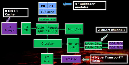
The System Request Queue and Crossbar modules shown in the diagram are the real brains behind the new northbridge. They are charged with information traffic control, redirecting all of the information from their source to destination. The SRQ handles all the traffic and requests from module cores, L3 cache and APICs. It's interesting to know that SRQ can also process core requests from other processors in multisocket setups. Crossbar on the other hand deals with system memory and HyperTransport infromation flow. Together, these two modules ensure that the data needed will be on disposal in shortest possible time, without wasting any unnecessary bandwidth...that's the idea anyways.
The Zambezi processor has two memory controllers, supporting DDR3 only, and up to 1866 MHz speed in dual channel configuration. DDR3 1600 MHz is supported in four sticks configurations only, tough. Controllers support unbuffered, registered, and Load Reduced type of memories, working at 1.50 V, 1.35 V or 1.25 V. The memory controller received a heavy upgrade on the power management side, and now supports a whole variate of tips and tricks on how to eliminate any excess power usage.
Four HyperTransport links are also upgraded and are now running 5.2 GT/s, each 16 bit wide and can be split into two 8 bit links (multiprocessor configuration). The number of active links is dependent on the configuration in which Zambezi's core will be used. For the desktop market, only one HT link will be active, and will be used to communicate with the chipset. Other links are reserved for server specifications, where they will be used for processor to processor communication.
Our Patreon Silver Supporters can read articles in single-page format.
May 6th, 2024 22:19 EDT
change timezone
Latest GPU Drivers
New Forum Posts
- GPU Hot Spot Temperature 105 Celsius, fans at 3000 RPM, while GPU Temperature is max 70 Celsius (40)
- Cybersecurity - OSINT Software for Linux (3)
- Gigabyte Aorus Elite AX V2 rev 1.1 BIOS update "AMD AGESA V2 1.2.0.B" (5)
- nvflashk - Flash any BIOS to NVIDIA GPUs - Safe board ID bypass up to 4xxx series (241)
- Only some humans can see refresh rates faster than others, I am one of those humans. (201)
- The Official Thermal Interface Material thread (1167)
- RTX 2070 8GB unable to flash (0)
- Update on the whole PC rebooting issue. There was an extra standoff in the case, but now it's crashing even more (3)
- What's your latest tech purchase? (20449)
- Battery swap for cyberpower UPS (61)
Popular Reviews
- Finalmouse UltralightX Review
- Cougar Hotrod Royal Gaming Chair Review
- Meze Audio LIRIC 2nd Generation Closed-Back Headphones Review
- Upcoming Hardware Launches 2023 (Updated Feb 2024)
- ASRock NUC BOX-155H (Intel Core Ultra 7 155H) Review
- Corsair iCUE Link RX120 RGB 120 mm Fan Review
- AMD Ryzen 7 7800X3D Review - The Best Gaming CPU
- ASUS Radeon RX 7900 GRE TUF OC Review
- Montech Sky Two GX Review
- HYTE THICC Q60 240 mm AIO Review
Controversial News Posts
- Intel Statement on Stability Issues: "Motherboard Makers to Blame" (248)
- Windows 11 Now Officially Adware as Microsoft Embeds Ads in the Start Menu (167)
- AMD to Redesign Ray Tracing Hardware on RDNA 4 (165)
- Sony PlayStation 5 Pro Specifications Confirmed, Console Arrives Before Holidays (118)
- AMD's RDNA 4 GPUs Could Stick with 18 Gbps GDDR6 Memory (114)
- NVIDIA Points Intel Raptor Lake CPU Users to Get Help from Intel Amid System Instability Issues (106)
- AMD Ryzen 9 7900X3D Now at a Mouth-watering $329 (104)
- AMD "Strix Halo" Zen 5 Mobile Processor Pictured: Chiplet-based, Uses 256-bit LPDDR5X (103)