 28
28
ASUS ENGTS450 TOP DirectCU 1 GB Review
(28 Comments) »Introduction
Today NVIDIA launches their new GeForce GTS 450 Series of graphics cards. As the "GTS" naming suggests, the card is more of a mid-range part than a high-performance device. It is NVIDIA's expressed goal to offer a low priced DirectX 11 graphics card that the majority of gamers can afford - and still play the latest games.
Architecture

NVIDIA's GF106 GPU is based on NVIDIA's Fermi architecture, which was released earlier this year. In order to achieve the product performance and positioning NVIDIA was looking for, they disabled some components of the full GF106 core, resulting in the graphics processor for the GeForce GTS 450. Unlike other Fermi-class cards the changes here are quite limited. Basically NVIDIA removed two memory chips from the design, two chips less means 2x 32-bit less bus interface, so a single 64-bit memory controller got disabled. The memory bus width is closely coupled to the number of active ROPs in the GPU, so one ROP partition is also disabled. Overall this change enables board partners to build more price competitive products because of the reduced cost for memory chips and PCB signal routing. It helps NVIDIA to increase its GPU yields. This also leaves NVIDIA with the option to create a more powerful "GTS 455" SKU at a later time, that has a 192-bit GDDR5 memory interface, with likely 768 MB or 1536 MB of memory.
It's interesting to note that NVIDIA did not disable any of the streaming multiprocessor units (SMs), and all four SMs holding 48 CUDA cores each are enabled, giving the CUDA core count of 192. NVIDIA's reference clocks on the GeForce GTS 450 are fairly low with 783 MHz core, 1566 MHz CUDA cores, and 900 MHz memory, so it comes as no surprise that most board partners are shipping pre-overclocked cards at lauch.
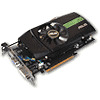
The ASUS ENGTS 450 TOP DirectCU that we have on our test bench today is a factory overclocked version that comes at substantially increased clocks compared to the reference design: 925 MHz vs. 783 MHz. As cooling solution ASUS' DirectCU cooler is used which we have seen on a variety of other recent cards from ASUS.
| Radeon HD 4850 | GeForce GTS 250 | Radeon HD 5750 | GeForce GTS 450 | ASUS GTS 450 TOP | Radeon HD 4870 | Radeon HD 5770 | GeForce | GeForce GTX 460 | Radeon HD 5830 | GeForce GTX 275 | GeForce GTX 460 | |
| Shader units | 800 | 128 | 720 | 192 | 192 | 800 | 800 | 216 | 336 | 1120 | 240 | 336 |
| ROPs | 16 | 16 | 16 | 16 | 16 | 16 | 16 | 28 | 24 | 16 | 28 | 32 |
| GPU | RV770 | G92 | Juniper | GF106 | GF106 | RV770 | Juniper | GT200 | GF104 | Cypress | GT200 | GF104 |
| Transistors | 956M | 754M | 1040M | 1170M | 1170M | 956M | 1040M | 1400M | 1950M | 2154M | 1404M | 1950M |
| Memory Size | 512 MB | 1024 MB | 1024 MB | 1024 MB | 1024 MB | 512 MB | 1024 MB | 896 MB | 768 MB | 1024 MB | 896 MB | 1024 MB |
| Memory Bus Width | 256 bit | 256 bit | 128 bit | 128 bit | 128 bit | 256 bit | 128 bit | 448 bit | 192 bit | 256 bit | 448 bit | 256 bit |
| Core Clock | 625 MHz | 738 MHz | 700 MHz | 783 MHz | 925 MHz | 750 MHz | 850 MHz | 576 MHz | 675 MHz | 800 MHz | 602 MHz | 675 MHz |
| Memory Clock | 993 MHz | 1100 MHz | 1150 MHz | 900 MHz | 1000 MHz | 900 MHz | 1200 MHz | 999 MHz | 900 MHz | 1000 MHz | 1107 MHz | 900 MHz |
| Price | $95 | $110 | $125 | $129 | $139 | $135 | $140 | $180 | $170 | $190 | $230 | $230 |
Packaging

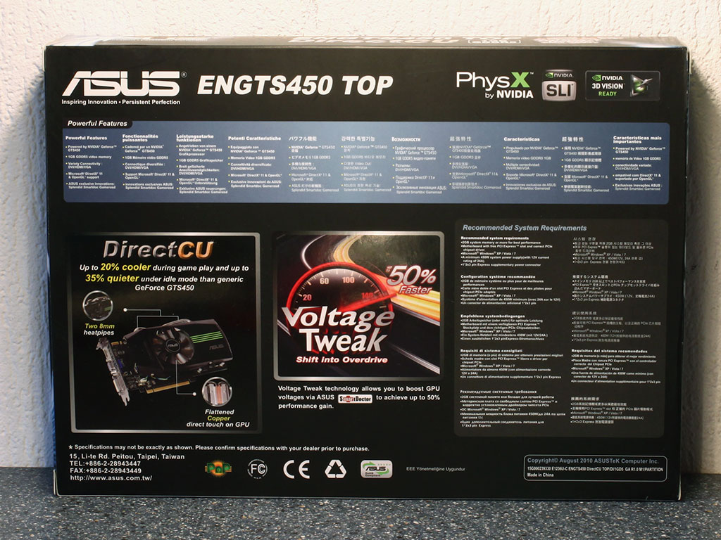
Umm.. a Tiger-Man-Eagle thing on the front of the package? Whatever .. the front of the package emphasizes the "925 MHz" clock speed very nicely and also mentions the puny 783 MHz the reference design runs at, good job here, ASUS.
Contents
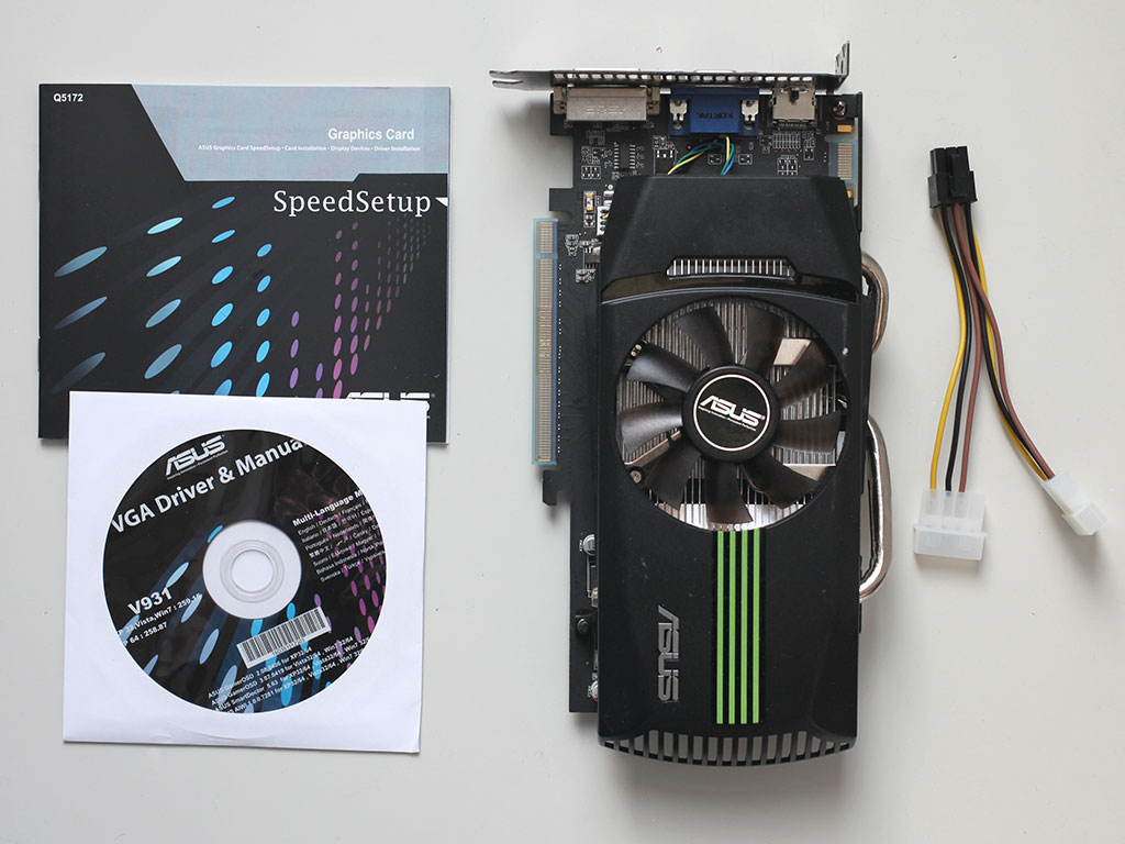
You will receive:
- Graphics card
- Driver CD
- Quick Install Guide
- PCI-Express power adapter
Our Patreon Silver Supporters can read articles in single-page format.
Apr 29th, 2024 13:03 EDT
change timezone
Latest GPU Drivers
New Forum Posts
- Why MS buying all of these Studios is bad for Gaming (50)
- Is this Sapphire PULSE RX 5600 XT legit or fake? (0)
- Arctic MX-6 shelf life is just a couple months? (14)
- New High Performance, x86 Compatible Microprocessors from Centaur / VIA (146)
- PL1 | OMEN 17-cb0xxx / I7-9750H / RTX 2060 (4)
- Z790 ACE MAX? (5)
- Dialing in the overlock on my new 12600kf, matured silicon process showing great results... (17)
- Is it better for zero RPM PSUs to place the fan on top? (21)
- What's your latest tech purchase? (20391)
- All I want is 2 monitors + 1 PC - Help! (2)
Popular Reviews
- Ugreen NASync DXP4800 Plus Review
- HYTE THICC Q60 240 mm AIO Review
- Upcoming Hardware Launches 2023 (Updated Feb 2024)
- MOONDROP x Crinacle DUSK In-Ear Monitors Review - The Last 5%
- FiiO K19 Desktop DAC/Headphone Amplifier Review
- Thermalright Phantom Spirit 120 EVO Review
- ASUS Radeon RX 7900 GRE TUF OC Review
- AMD Ryzen 7 7800X3D Review - The Best Gaming CPU
- Logitech G Pro X Superlight 2 Review - Updated with 4000 Hz Tested
- ASUS GeForce RTX 4070 Ti Super TUF Review
Controversial News Posts
- Windows 11 Now Officially Adware as Microsoft Embeds Ads in the Start Menu (146)
- Intel Statement on Stability Issues: "Motherboard Makers to Blame" (139)
- Sony PlayStation 5 Pro Specifications Confirmed, Console Arrives Before Holidays (117)
- NVIDIA Points Intel Raptor Lake CPU Users to Get Help from Intel Amid System Instability Issues (106)
- AMD "Strix Halo" Zen 5 Mobile Processor Pictured: Chiplet-based, Uses 256-bit LPDDR5X (103)
- AMD's RDNA 4 GPUs Could Stick with 18 Gbps GDDR6 Memory (99)
- US Government Wants Nuclear Plants to Offload AI Data Center Expansion (98)
- TechPowerUp Hiring: Reviewers Wanted for Motherboards, Laptops, Gaming Handhelds and Prebuilt Desktops (89)