 141
141
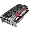
ASUS Radeon R9 Fury STRIX 4 GB Review
(141 Comments) »Introduction
Two weeks following its flagship Radeon R9 Fury X launch, AMD is launching its little sibling, the R9 Fury, positioned as a big money-maker for the "Fiji" silicon. To say AMD is at the forefront of new technology is an understatement. The company rigorously pursues and in many cases introduces new technology into the PC consumer-graphics space. AMD's past two memorable technological breakthroughs in this space were Graphics CoreNext, a powerful new number-crunching machinery for the GPU, which made not just AMD, but also a lot of crypto-currency enthusiasts a lot of money, and GDDR5 memory in their giant-killing Radeon HD 4870. The past year hasn't been kind to AMD in terms of GPU-market share, which is partly because the company didn't introduce anything major since 2013; all due to competition from NVIDIA with its "Maxwell" architecture and probably also because the company is focusing on high-volume ISV deals, such as new-generation game consoles, and the development of the chip that drives the card we're reviewing today, the Radeon R9 Fury.

Unlike the R9 Fury X, this SKU doesn't have a defined reference-design. AMD is allowing its board partners to go to town with it. To make it as affordable as possible, conventional air-based cooling solutions are used. At this time, there are only two board partners offering this card, ASUS and Sapphire. This is surprising because the chip has the potential to not only outsell the R9 Fury X, but also sell in reasonable volumes against NVIDIA's competing products.
The card we're reviewing today is the ASUS Radeon R9 Fury STRIX. It features the company's new-generation DirectCU III triple-fan cooling solution, which made its debut with the R9 390X and GTX 980 Ti. Let's tell you up front that it's quieter than the R9 Fury X in idle because it turns its fans off. ASUS decided to not overclock their card, but is still asking a $30 price premium over AMD's MSRP.
| GeForce GTX 970 | Radeon R9 290X | Radeon R9 390X | GeForce GTX 780 Ti | GeForce GTX 980 | Radeon R9 Fury | ASUS R9 Fury Strix | Radeon Fury X | GeForce GTX 980 Ti | |
|---|---|---|---|---|---|---|---|---|---|
| Shader Units | 1664 | 2816 | 2816 | 2880 | 2048 | 3584 | 3584 | 4096 | 2816 |
| ROPs | 56 | 64 | 64 | 48 | 64 | 64 | 64 | 64 | 96 |
| Graphics Processor | GM204 | Hawaii | Hawaii | GK110 | GM204 | Fiji | Fiji | Fiji | GM200 |
| Transistors | 5200M | 6200M | 6200M | 7100M | 5200M | 8900M | 8900M | 8900M | 8000M |
| Memory Size | 4096 MB | 4096 MB | 8192 MB | 3072 MB | 4096 MB | 4096 MB | 4096 MB | 4096 MB | 6144 MB |
| Memory Bus Width | 256 bit | 512 bit | 512 bit | 384 bit | 256 bit | 4096 bit | 4096 bit | 4096 bit | 384 bit |
| Core Clock | 1051 MHz+ | 1000 MHz | 1050 MHz | 876 MHz+ | 1126 MHz+ | 1000 MHz | 1000 MHz | 1050 MHz | 1000 MHz+ |
| Memory Clock | 1750 MHz | 1250 MHz | 1500 MHz | 1750 MHz | 1750 MHz | 500 MHz | 500 MHz | 500 MHz | 1750 MHz |
| Price | $310 | $300 | $430 | $390 | $480 | $549 | $579 | $650 | $650 |
Architecture
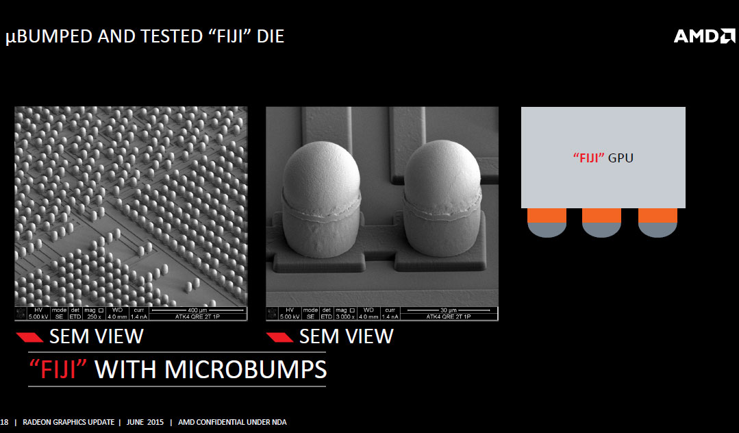
At the heart of the Radeon R9 Fury is the most talked about GPU of the season, codenamed "Fiji." It is a multi-chip module out of three important components—the GPU die itself, built on TSMC's 28 nm process, a specially designed silicon substrate layer that seats and connects the GPU die with the HBM memory stacks called interposer and built by UMC on its 65 nm process, and four 1 GB HBM stacks made by SK Hynix on a 20 nm-class node. AMD had technical assistance from some of the industry's brightest VLSI teams, including from UMC, Amkor Technology, ASE Group, and SK Hynix.Let's begin with the GPU die itself. It features a familiar component hierarchy to the previous-generation "Hawaii" silicon. The Graphics CoreNext stream processors, however, are of a newer generation, GCN 1.2, which made its debut with the "Tonga" silicon that powers the Radeon R9 380 and R9 285. As we mentioned before, AMD created the R9 Fury by disabling a few components on the "Fiji" silicon. Those disabled components are shaded red in the architecture diagram below.
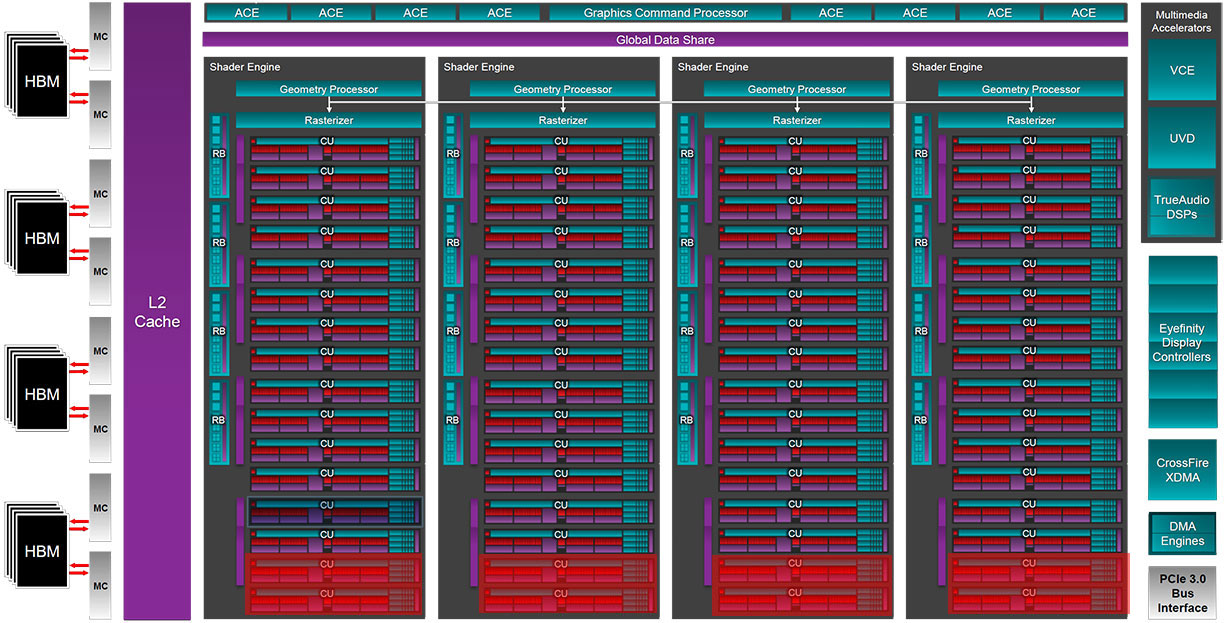
The GPU die features four shader engines, just like "Hawaii," but the compute unit (CU) count per shader engine has been increased to 14 from the 11 on "Hawaii." Each CU packs 64 stream processors, so there are 896 stream processors per engine and 3,584 on the chip in total. There are 16 render back-ends, which is the same as with "Hawaii," so the ROP count is the same at 64. The higher CU count, however, means that the TMU count is at 224 instead of the 176 on "Hawaii." The biggest change, however, is the 4096-bit wide HBM interface that wires out to four 8 Gigabit HBM stacks. AMD carved the R9 Fury out of the "Fiji" silicon by enabling 56 of the 64 compute units.
AMD didn't announce any changes to the ancillaries—the multimedia engine, XDMA CrossFire (no bridge cables required), display controllers with support for DisplayPort 1.2a and HDMI 1.4a, and PCI-Express gen 3.0 x16 host interface remain the same as on "Hawaii." There is one notable change, though, since the reference design card lacks DVI connectors. It features a HDMI and three DP 1.2a ports. All ports are on the first slot elevation, making this card truly single-slot capable with aftermarket liquid-cooling blocks (the piggybacked DVI connector that extends into the second slot denies NVIDIA cards this cool feature unless you're skillful enough to solder out the DVI connector without accidentally shorting any pins).
High Bandwidth Memory and Interposer
With Windows 10 and its companion DirectX 12 API on the horizon and high display resolutions such as 1440p and 4K Ultra HD getting increasingly more affordable—1440p displays start at $250 and 4K starts at $400 if you know where to look—the demands on video memory to catch up have never been higher. GDDR5 served the industry well since its debut in 2008. It has driven five generations of GPUs since, but is approaching its design limitation for performance upscaling through clock-speed increases.

For any memory standard (including HBM), memory speed/bandwidth and power draw don't scale linearly. Beyond a point, the equation tapers too much in favor of power requirements, and so, an increasingly disproportionate amount of power is required to achieve higher clocks. This is what necessitates a new memory standard. HBM is just starting out on that same curve, and has, hence, much better energy efficiency than GDDR5. HBM trades frequency for bus-width and offers vertical stacking of DRAM dies. This generation of HBM allows vertical stacking of up to four DRAM dies, with a fifth logic die holding the PHY and connections of the stack.
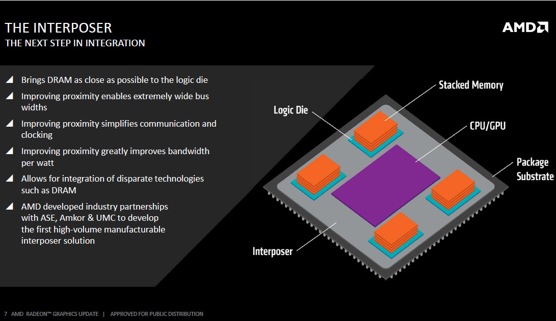
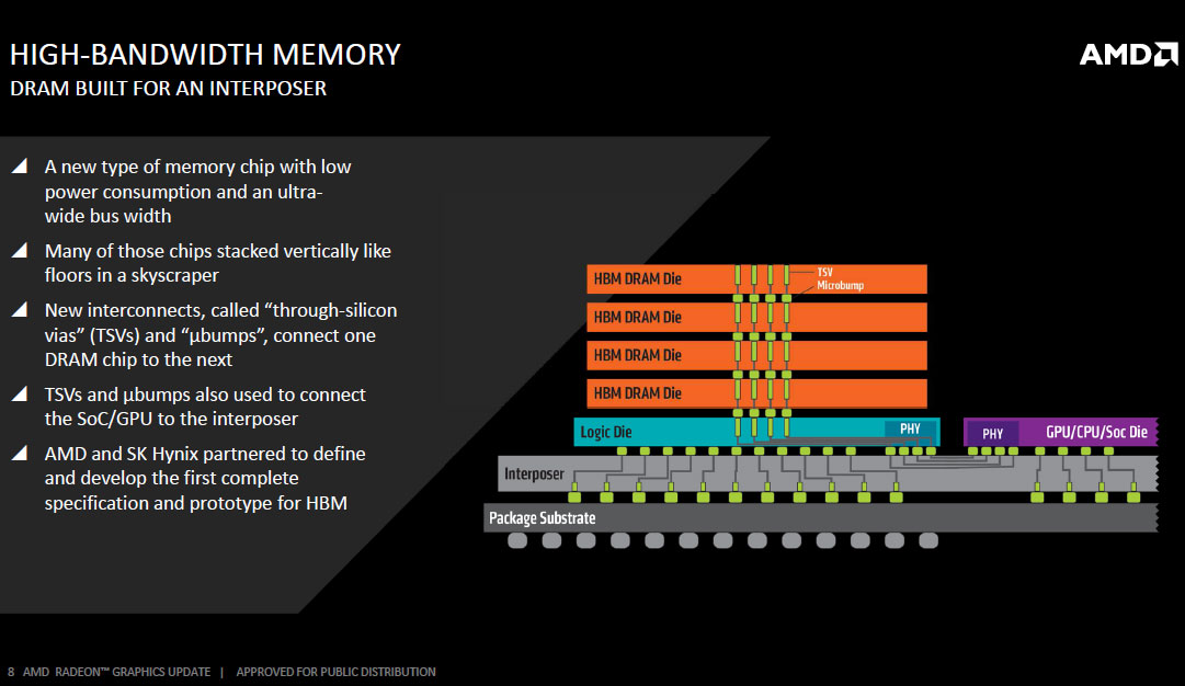
The Fiji package features four 8 Gb HBM stacks, each with 1,024-bit wide memory bus. Since such a wide bus per stack would take up an obscene number of pins on a standalone memory chip package, AMD decided to integrate it into the GPU package, using a specially designed substrate called the interposer to deal with the wiring problem.
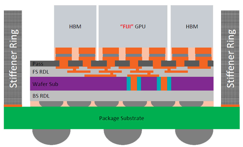
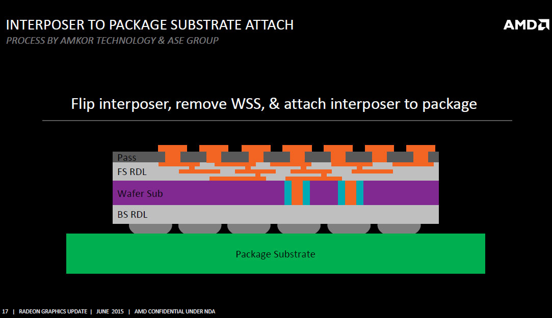
The interposer is essentially a very large silicon die that acts as a substrate for other dies. There's no number crunching or storage happening here as there is just a vast network of microscopic wires running between the HBM stacks and the GPU die. The interposer is built on a 65 nanometer silicon fab node. It may not sound like much in the 20 nm-class era, but compared to conventional fiberglass PCB wiring, wires on the 65 nm node are infinitesimally smaller, as are bumps, points of contact between two dies or between a die and a substrate. AMD innovated microscopic bumps specifically for contact between the GPU die and the interposer because wiring between the GPU and the memory is just so dense.

The interposer has microscopic bumps on the side that faces toward the GPU die and HBM stacks and conventional bumps, also on the side, that face toward the main fiberglass substrate of the GPU package. With the memory moved to the GPU package, and more importantly, the most sensitive wiring of the video card (that between the memory and GPU) moved to the GPU package, there's not much action on the PCB. The pins on the package are for power, system bus, and display I/O, which gives AMD greater quality control.


Another major benefit of moving the memory to the GPU package, however, is the savings in PCB real-estate. Sure, the package in itself is bigger than "Hawaii" or any GPU ever made, but since there are no memory chips surrounding it, all that's left on the video card's PCB are the GPU package, VRM, and display I/O. This allows AMD to create some extremely compact products. Unlike the reference R9 Fury X, the ASUS R9 Fury STRIX, however, offers a conventionally sized PCB. Despite the meaty VRM, you can still see large empty areas on the PCB.
Packaging

Our Patreon Silver Supporters can read articles in single-page format.
Jun 30th, 2025 18:13 CDT
change timezone
Latest GPU Drivers
New Forum Posts
- Will you buy a RTX 5090? (581)
- The TPU UK Clubhouse (26529)
- Do you use Linux? (663)
- Can you guess Which game it is? (194)
- Help me choose the right PSU , Cooler Master vs Seasonic (53)
- HOW TO ADD NVMe M.2 SSD SUPPORT TO OLD MOTHERBOARDS WITH AWARD-Phoenix LEGACY SUPPORT? (2)
- Whats a fair asking price - MSI 4070 Super (4)
- HTPC Power Consumption Discussion, Upgrade vs Migration (18)
- RX 9000 series GPU Owners Club (1103)
- Rare GPUs / Unreleased GPUs (2111)
Popular Reviews
- Sapphire Radeon RX 9070 XT Nitro+ Review - Beating NVIDIA
- ASUS ROG Crosshair X870E Extreme Review
- Sapphire Radeon RX 9060 XT Pulse OC 16 GB Review - Samsung Memory Tested
- Lexar NQ780 4 TB Review
- AVerMedia CamStream 4K Review
- ASRock Phantom Gaming Z890 Riptide Wi-Fi Review
- AMD Ryzen 7 9800X3D Review - The Best Gaming Processor
- Upcoming Hardware Launches 2025 (Updated May 2025)
- Intel Core Ultra 7 265K Review
- NVIDIA GeForce RTX 5060 8 GB Review
TPU on YouTube
Controversial News Posts
- Intel's Core Ultra 7 265K and 265KF CPUs Dip Below $250 (288)
- NVIDIA Grabs Market Share, AMD Loses Ground, and Intel Disappears in Latest dGPU Update (204)
- Some Intel Nova Lake CPUs Rumored to Challenge AMD's 3D V-Cache in Desktop Gaming (140)
- Microsoft Partners with AMD for Next-gen Xbox Hardware (105)
- NVIDIA Launches GeForce RTX 5050 for Desktops and Laptops, Starts at $249 (104)
- Intel "Nova Lake‑S" Series: Seven SKUs, Up to 52 Cores and 150 W TDP (100)
- NVIDIA GeForce RTX 5080 SUPER Could Feature 24 GB Memory, Increased Power Limits (89)
- Reviewers Bemused by Restrictive Sampling of RX 9060 XT 8 GB Cards (88)