 114
114
ASUS Radeon HD 6990 4 GB Review
Test Setup »A Closer Look


AMD is using a big and complex heatsink which cools all components at the same time: GPU 1, GPU 2, memory of both GPUs, voltage regulation circuitry and the PCI-Express bridge chip. AMD claims to use a special "phase change" thermal interface material, and they say once removed you will not be able to get the same temperatures with your own TIM. If you take a close look at the second picture you can see that the paste is not liquid, but more like brittle wax.


This little switch is present on the HD 6950 and HD 6970 cards, too. Originally it was designed as a backup feature, so you have a second BIOS in case you manage to destroy your main BIOS.
AMD has changed the behaviour on the HD 6990 and turned it into an overclocking feature. When left in the default position, the card uses the normal settings of 830 MHz core and 1.12 V GPU voltage. When set to the second position, the card will use a BIOS that's clocked at 880 MHz core and 1.175 V. The switch is covered by a scary big, yellow sticker which basically tells you that switching the BIOS will void your warranty.
During production AMD does a "bootup" test at the overclocked settings, but they do not guarantee stability of the card in this mode. The sticker itself did not pose a big problem, it can be removed, moved and put back easily.
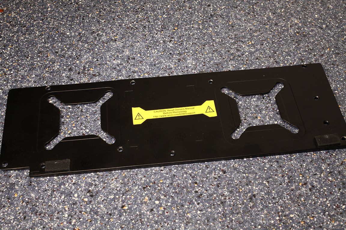

The backplate is made from metal and serves to protect the components on the back from damage. It also helps with cooling the memory chips and acts as a general heatspreader. Warning: This plate gets quite hot when the card is heavily loaded. I moved the yellow sticker from the switch to the middle of the backplate where it's hard to lose, still visible and out of the way.

The card requires two 8-pin PCI-Express power connectors. Together with the PCI-Express x16 slot this configuration is good for 375 W of power - AMD says their board can draw up to 375 W in "normal" mode and up to 450 W when overclocked.

The GDDR5 memory chips are made by Hynix, and carry the model number H5GQ2H24MFR-T2C. They are specified to run at 1250 MHz (5000 MHz GDDR5 effective).

AMD is using two Volterra's VT1556 voltage controllers on their HD 6990 (one for each GPU). The VT1556 is also present on the reference designs for HD 6950 and HD 6970.

The PCI-Express bridge chip which connects the two GPUs and interfaces with the system via PCI-Express 2.0 is made by PLX. Apparently PLX lets ATI rebrand their product. According to AMD the bridge chip supports PCI-Express 2.1 x16 which supplies enough bandwidth to both GPUs for any situation. This is the same bridge chip as used on the Radeon HD 5970.

AMD's new Cayman graphics processor is made on a 40 nm process at TSMC Taiwan. It uses approximately 2.64 billion transistors on a die area of 389 mm².
May 8th, 2024 14:20 EDT
change timezone
Latest GPU Drivers
New Forum Posts
- not impressed - nvme vs ssd (63)
- Last game you purchased? (265)
- POLL: Can you see the difference past 60fps (gaming/other) (51)
- PSU making a clicking sound, PC wont turn on (26)
- Epic Games launcher's ridiculous CPU usage (23)
- Does anyone here overclock their video cards? Is it really worth it? (67)
- Your way of cooling your PC? (31)
- Only some humans can see refresh rates faster than others, I am one of those humans. (224)
- Urgent: PC wont turn on with PSU connected to MOBO (25)
- What are you playing? (20600)
Popular Reviews
- CHERRY XTRFY M64 Pro Review
- Corsair iCUE Link RX120 RGB 120 mm Fan Review
- Finalmouse UltralightX Review
- Upcoming Hardware Launches 2023 (Updated Feb 2024)
- Cougar Hotrod Royal Gaming Chair Review
- Bykski CPU-XPR-C-I CPU Water Block Review - Amazing Value!
- Meze Audio LIRIC 2nd Generation Closed-Back Headphones Review
- AMD Ryzen 7 7800X3D Review - The Best Gaming CPU
- ASRock NUC BOX-155H (Intel Core Ultra 7 155H) Review
- ASUS Radeon RX 7900 GRE TUF OC Review
Controversial News Posts
- Intel Statement on Stability Issues: "Motherboard Makers to Blame" (261)
- AMD to Redesign Ray Tracing Hardware on RDNA 4 (205)
- Windows 11 Now Officially Adware as Microsoft Embeds Ads in the Start Menu (167)
- NVIDIA to Only Launch the Flagship GeForce RTX 5090 in 2024, Rest of the Series in 2025 (142)
- Sony PlayStation 5 Pro Specifications Confirmed, Console Arrives Before Holidays (119)
- AMD's RDNA 4 GPUs Could Stick with 18 Gbps GDDR6 Memory (114)
- NVIDIA Points Intel Raptor Lake CPU Users to Get Help from Intel Amid System Instability Issues (106)
- AMD Ryzen 9 7900X3D Now at a Mouth-watering $329 (104)