 88
88
Intel Core i9-10900 Review - Fail at Stock, Impressive when Unlocked
Test Setup »Architecture
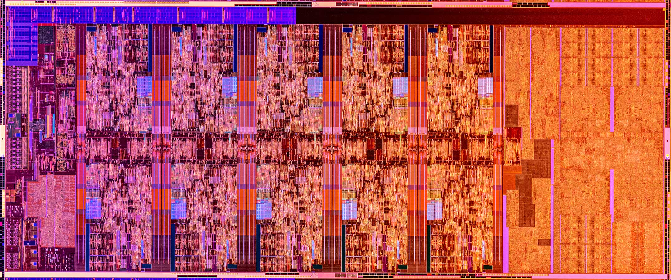
Under the hood of the Core i9-10900 is the 10-core "Comet Lake-S" silicon built on the same 14 nm++ process as the previous two generations, but with a key difference.

Intel physically thinned the die along the Z-axis by removing as much of the silicon bulk as possible, with the idea being that heat generated by the die travels through less silicon. The more conductive copper integrated heatspreader has been made thicker, and a solder thermal interface material (STIM) is used between the two. The die area is estimated by AnandTech to be around 198.4 mm², and from the looks of it, Intel can't add any more cores on this package by stretching the die without chopping off the iGPU.
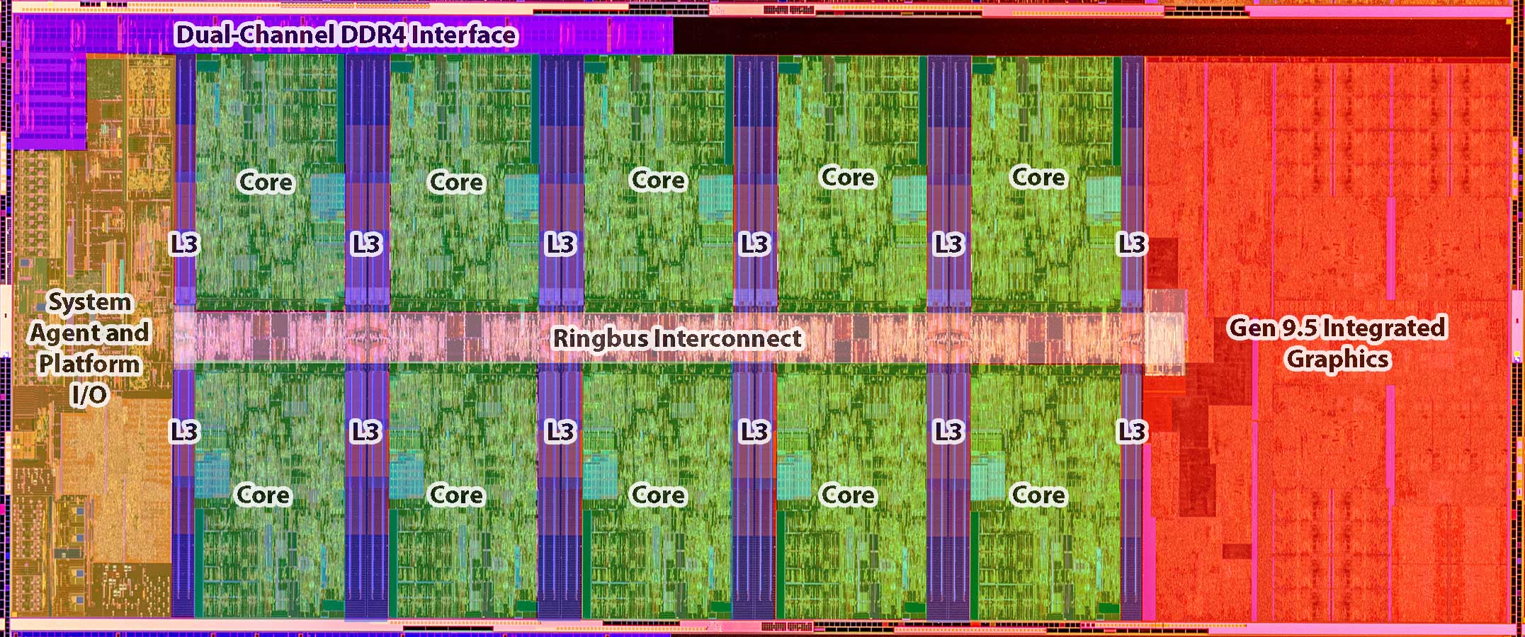
The "Comet Lake-S" silicon is laid out similar to the past four generations of Intel mainstream processors, with two rows of CPU cores flanked by the iGPU on one side and the system agent (integrated northbridge) on the other, and a Ringbus Interconnect serving as town square between the various components. The last-level cache is scattered across as slices, adding up to 20 MB of unified L3 cache all cores can access equally.
Much of the processor's uncore components are clumped into the system agent, which contains the memory controller, PCI-Express gen 3.0 root-complex, DMI interface, and memory PHY. The iGPU solution, although present on the silicon, is permanently disabled by Intel. On the other end of the ringbus is the Gen 9.5 integrated graphics, which has practically been carried over for the past three generations, featuring 24 execution units in the GT2 trim. All SKUs in the desktop 10th Gen processor series appear to have the top GT2 trim. Don't expect to play PUBG at 4K on this; the "UHD" moniker only indicates that the IGP can handle 4K Ultra HD displays, features modern connectivity options, such as DP 1.4 and HDMI 2.0, and can playback 4K video in new formats with 10-bpc color and HDR10/Dolby Vision standards.
The core itself is identical in design to "Skylake," and there are hence no IPC increases to be had. As we explained in the introduction, all of Intel's efforts to increase gaming, single-threaded, and less-parallelized application performance revolve around increasing clock speeds and deploying as many as three intelligent boosting algorithms to achieve the advertised clock speeds.
Boost Algorithms
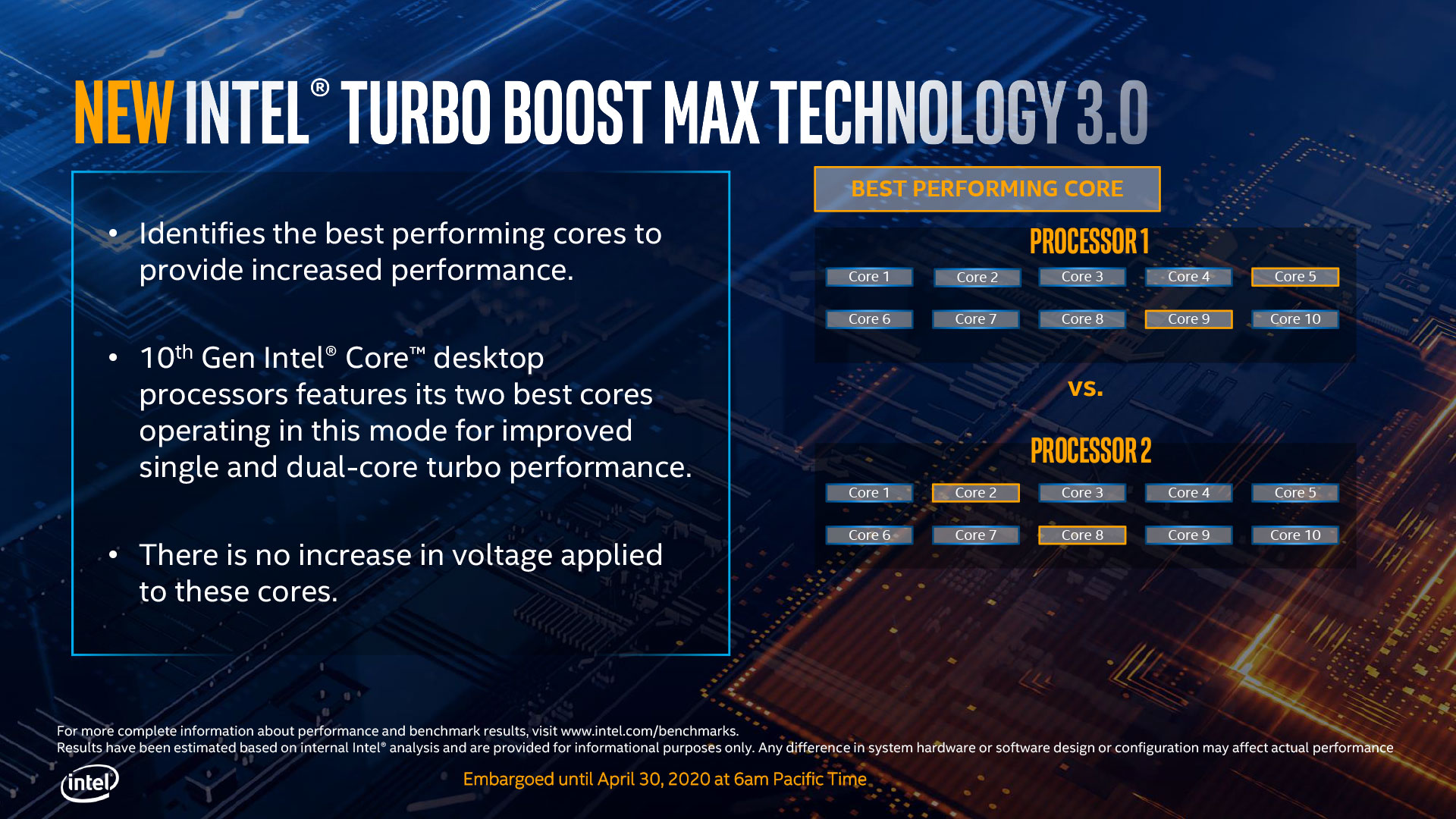
The Core i9-10900 has a nameplate base frequency (aka nominal clock) of 2.80 GHz. The processor embarks on a fascinating journey toward 5.20 GHz from here. The processor leverages Turbo Boost 2.0 to raise clock speeds up to 5.00 GHz, with varying boost multipliers along the way to workloads scaling across multiple cores. Beyond this, the Turbo Boost Max 3.0 algorithm, carried over from the company's Core X HEDT processors, is engaged. The algorithm raises frequencies of the processor's two favored cores up to 5.10 GHz. Beyond this, the processor invokes Thermal Velocity Boost, a brand-new algorithm that opportunistically overclocks the processor to 5.20 GHz in short bursts provided the processor's cooling solution is effective (able to keep temperatures below 70°C), and the processor's power budget permitting.
With "Comet Lake," Intel is introducing favored cores to its mainstream desktop processor segment, which was until now restricted to its HEDT and server processors. AMD supports this tech across its Zen product stack. Two of the best-performing cores on the silicon are identified at the time of each die's manufacturing, their information is hardcoded. Favored cores-aware operating systems (Windows 1709 or later and Linux kernels since January 2018) are able to identify this information, and send the most traffic to these two cores as they are able to sustain boost frequencies the best.
PL1, or power level one, spreads a 65 W power budget to support them across a default 28-second Tau (a time value for which the processor is allowed to sustain its boost frequencies before having to fall back to nominal clocks). PL2, on the other hand, is something else. Set at 224 W, motherboard manufacturers have been given the freedom to override PL2 and Tau as they see fit, so various motherboards implement power limits differently depending on the effectiveness of their VRM solution. You are hence rewarded for buying a pricier motherboard that has a better VRM coupled with a more aggressive vendor-supplied power management. Of course, all boards come with Intel-spec fallbacks. We will examine the boosting behavior at Intel spec and compare it with the "ASUS enhanced" specs of the ROG Maximus XII Extreme later on in this review.
Intel introduced a handful of overclocker-friendly features with the 10th generation, including the ability to toggle HyperThreading on a per-core basis rather than globally. This could be an interesting option for those gaming and streaming, where a certain number of cores have HTT disabled for the best gaming performance and certain cores have them enabled, with Windows process core affinity settings taking care of the rest.
The company also introduced the ability to overclock the DMI chipset bus. DMI is a PCIe-based interconnect that handles transfers between the processor and the chipset (PCH). The LGA1200 platform uses DMI 3.0 (comparable to PCI-Express 3.0 x4 in terms of bandwidth). Intel has apparently decoupled PCIe clock domains to enable you to overclock the DMI and PEG (that topmost x16 PCIe slot) without destabilizing your PCIe setup for graphics cards. Multiplier-based overclocking, however, isn't possible on the Core i9-10900.
The Z490, H470, and B460 Platforms
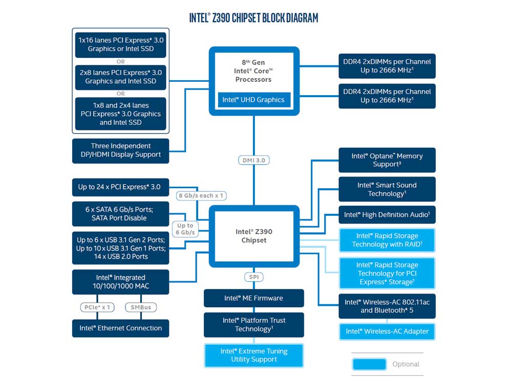
Z490 is the top 400-series chipset targeted at gaming desktops and PC enthusiasts, as it enables serious overclocking and multi-GPU support. In terms of I/O capabilities, the chipset is nearly identical to the Z390, with 24 downstream PCIe gen 3.0 lanes, six SATA ports, six USB 3.2 gen 2 ports that can be converted to three USB 3.2 gen 2x2 ports, ten USB 3.2 gen 1 ports, and fourteen USB 2.0 ports. Intel is recommending its i225-V 2.5 Gbps Ethernet chip as the wired networking solution to go with Z490, and the company's AX201 802.11ax WiFi 6 WLAN solution to go with the chipset's CNVio interface.
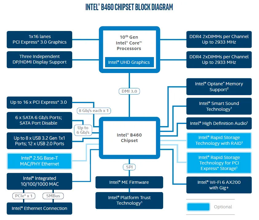

You are more likely to pair locked Intel Core processors with the B460 or H470 chipsets. B460 has motherboards start at around the $90 mark. It comes with 16 downstream PCIe gen 3.0 lanes (compared to just 12 on the previous-generation B360). Compared to Z490, you get fewer PCIe lanes (16 vs. 24) from the chipset, and fewer USB 3.2 ports (eight 5 Gbps ports and no 10 Gbps ports compared to six 10 Gbps and ten 5 Gbps ports on the Z490). You also lose out on CPU overclocking features and multi-GPU capabilities (such as SLI). B460 motherboards also come with memory frequency restrictions set to DDR4-2933. The H470 is an interesting middle ground between the Z490 and B460. You still lose out on multi-GPU and overclocking, but get more platform PCIe lanes (20 vs. 16 on the B460 and 24 on the Z490), as well as four 10 Gbps USB 3.2 ports in addition to what you get from the B460.
Despite being a multiplier-locked chip, we'd still recommend you check out at least a mid-range Z490 chipset motherboard to benefit from unlocked memory clocks, power limit flexibility, and good enough CPU VRM solutions.
Jun 14th, 2024 11:07 EDT
change timezone
Latest GPU Drivers
New Forum Posts
- What are you playing? (20827)
- Good Bronze 750w PSU (80)
- Bios rookit? (11)
- how can i connect this little passive sub to a very simple stereo amp (12)
- Buy a Deepcool cooler? Go to Prison! (0)
- What's your latest tech purchase? (20791)
- MSI CPU Force (3)
- Acer Nitro 5 Extreme Overheating - Tried Everything, Don't Know What To Do (14)
- Anime Nation (12811)
- Is the ThermalRight Frozen Prism 360 AIO good? (91)
Popular Reviews
- VAXEE Outset AX Wireless (4K) Review
- Pulsar Xlite V3 eS Review
- Upcoming Hardware Launches 2024 (Updated May 2024)
- Aune AR5000 Headphones + S17 Pro Headphones Amplifier Review
- Intel Lunar Lake Technical Deep Dive - So many Revolutions in One Chip
- AMD Ryzen 7 7800X3D Review - The Best Gaming CPU
- Quick Look: Final UX2000 Wireless Noise Canceling Headphones
- NZXT H6 Flow RGB Review
- Pulsar Xlite V3 Review
- Thermal Grizzly KryoSheet Review - Tested on RX 7900 XTX with 475 W
Controversial News Posts
- Possible Specs of NVIDIA GeForce "Blackwell" GPU Lineup Leaked (131)
- NVIDIA RTX 5090 "Blackwell" Founders Edition to Implement the "RTX 4090 Ti" Cinderblock Design (118)
- Nightmare Fuel for Intel: Arm CEO Predicts Arm will Take Over 50% Windows PC Market-share by 2029 (105)
- AMD Zen 5 Storms into Gaming Desktops with Ryzen 9000 "Granite Ridge" Processors (100)
- Biden Administration to Revive Trump-Era Tariffs on China-made GPUs and Motherboards (95)
- ASRock Innovates First AMD Radeon RX 7000 Graphics Card with 12V-2x6 Power Connector (94)
- AMD Ryzen 9000 Zen 5 Single Thread Performance at 5.80 GHz Found 19% Over Zen 4 (92)
- AMD Outs Ryzen 5000XT Processors for Socket AM4, an 8-year Old Socket (84)