 509
509
NVIDIA GeForce RTX 4090 Founders Edition Review - Impressive Performance
(509 Comments) »Introduction
NVIDIA GeForce RTX 4090 "Ada Lovelace" turns the page, introducing a new generation of graphics hardware that promises not just fast gaming performance, but also makes real time ray tracing practically "free." In this RTX 4090 Founders Edition review we'll see that besides a big generational performance uplift, Ada also promises revolutionary improvements to NVIDIA's DLSS capability—generating entire frames only using AI, without involving the GPU's main graphics rendering machinery. This in itself is so significant, that the company is referring to it as "neural rendering," and placing it alongside the two other key graphics rendering techniques—rasterization and ray tracing. With the new GeForce RTX 4090, NVIDIA is promising a generational performance uplift of the kind we were seeing when Moore's Law still worked for GPUs—nearly 50% generation over generation.

The GeForce "Ada" graphics architecture, named after Ada Lovelace, considered to be the first computer programmer; heralds the 3rd generation RTX real time ray tracing technology, which combines classic raster graphics with certain real-time ray traced elements to significantly improve visual realism. Generationally, Ada enables visual artists and game developers to add even more ray traced effects to their games, and introduces new fixed function hardware to render them. The "Ada" CUDA cores in addition to significant frequency and IPC uplifts over "Ampere," introduce Shader Execution Reordering, a new SIMD optimization that improves the performance of the shader-side of ray tracing by three times, and in-game framerates by 25%. Ada also introduces the 4th generation Tensor Cores, with support for even more math formats such as FP8, improving tensor math performance uplifts by five times over the previous generation. Bringing this all together is the new TSMC 5 nm EUV foundry node that is capable of GPU clock speeds as high as 4 GHz for this generation.
NVIDIA carved the GeForce RTX 4090 out of the 5 nm "AD102" silicon, its largest for this generation. It is endowed with a massive 16,384 CUDA cores (out of 18,432 present on the silicon), 512 out of 568 Tensor cores, 128 out of 142 RT cores, 512 TMUs and 192 ROPs. The card uses the same 24 GB of GDDR6X memory as the RTX 3090, which ticks at the same 21 Gbps speed as the RTX 3090 Ti, producing 1008 GB/s of bandwidth. There are several innovations made at the silicon level, which we'll detail on the next page of this review; enabling NVIDIA to actually generationally lower the memory bandwidth, as you'll see in the RTX 4080 series, and the other SKUs from this generation.
The GeForce RTX 4090 is NVIDIA's flagship graphics card for this generation. The company is changing the launch order this time. With the RTX 30-series, NVIDIA launched the RTX 3080 as flagship first, and added the RTX 3090 / 3090 Ti later, as a halo product to replace the TITAN. With Ada, the RTX 4090 debuts this generation, with the RTX 4080 series slated for November 2022. The RTX 40-series launches in an interesting time in the market—cryptocurrency mining is dead, and with it, demand for high-margin flagship GPUs from miners. The PC industry is in a state of slump due to weakened demand; most of the tech industry is trading red; and people's disposable incomes are strained. NVIDIA is positioning the RTX 4090 at $1,599 (baseline MSRP), and pricing for most custom-design boards should be within a few hundred Dollars.
The NVIDIA GeForce RTX 4090 Founders Edition in this review follows a long line of well-designed graphics cards by NVIDIA that are technically custom-design, but are de-facto reference. With this generation, NVIDIA improves upon the Dual Axial Flow Through cooling architecture it introduced with the RTX 30-series "Ampere." While the GPU uses a PCI-Express Gen 4 host interface, its power architecture meets the PCIe Gen 5 standard, with the new 12+4 pin ATX 12VHPWR power connector being standardized across the RTX 4090 series, including with custom-design cards from partners. NVIDIA is placing the RTX 4090 at the baseline price of $1,599. This is the only card we are allowed to publish reviews of today (October 11), you'll have to check back tomorrow for reviews of custom-design 4090s—we'll test eight models, from all the big manufacturers.
| Price | Cores | ROPs | Core Clock | Boost Clock | Memory Clock | GPU | Transistors | Memory | |
|---|---|---|---|---|---|---|---|---|---|
| RTX 2080 | $400 | 2944 | 64 | 1515 MHz | 1710 MHz | 1750 MHz | TU104 | 13600M | 8 GB, GDDR6, 256-bit |
| RTX 3060 Ti | $450 | 4864 | 80 | 1410 MHz | 1665 MHz | 1750 MHz | GA104 | 17400M | 8 GB, GDDR6, 256-bit |
| RX 6700 XT | $410 | 2560 | 64 | 2424 MHz | 2581 MHz | 2000 MHz | Navi 22 | 17200M | 12 GB, GDDR6, 192-bit |
| RX 6750 XT | $470 | 2560 | 64 | 2495 MHz | 2600 MHz | 2250 MHz | Navi 22 | 17200M | 12 GB, GDDR6, 192-bit |
| RTX 2080 Ti | $550 | 4352 | 88 | 1350 MHz | 1545 MHz | 1750 MHz | TU102 | 18600M | 11 GB, GDDR6, 352-bit |
| RTX 3070 | $530 | 5888 | 96 | 1500 MHz | 1725 MHz | 1750 MHz | GA104 | 17400M | 8 GB, GDDR6, 256-bit |
| RTX 3070 Ti | $600 | 6144 | 96 | 1575 MHz | 1770 MHz | 1188 MHz | GA104 | 17400M | 8 GB, GDDR6X, 256-bit |
| RX 6800 | $580 | 3840 | 96 | 1815 MHz | 2105 MHz | 2000 MHz | Navi 21 | 26800M | 16 GB, GDDR6, 256-bit |
| RX 6800 XT | $600 | 4608 | 128 | 2015 MHz | 2250 MHz | 2000 MHz | Navi 21 | 26800M | 16 GB, GDDR6, 256-bit |
| RTX 3080 | $660 | 8704 | 96 | 1440 MHz | 1710 MHz | 1188 MHz | GA102 | 28000M | 10 GB, GDDR6X, 320-bit |
| RTX 3080 Ti | $850 | 10240 | 112 | 1365 MHz | 1665 MHz | 1188 MHz | GA102 | 28000M | 12 GB, GDDR6X, 384-bit |
| RX 6900 XT | $680 | 5120 | 128 | 2015 MHz | 2250 MHz | 2000 MHz | Navi 21 | 26800M | 16 GB, GDDR6, 256-bit |
| RX 6950 XT | $950 | 5120 | 128 | 2100 MHz | 2310 MHz | 2250 MHz | Navi 21 | 26800M | 16 GB, GDDR6, 256-bit |
| RTX 3090 | $950 | 10496 | 112 | 1395 MHz | 1695 MHz | 1219 MHz | GA102 | 28000M | 24 GB, GDDR6X, 384-bit |
| RTX 3090 Ti | $1200 | 10752 | 112 | 1560 MHz | 1950 MHz | 1313 MHz | GA102 | 28000M | 24 GB, GDDR6X, 384-bit |
| RTX 4090 | $1600 | 16384 | 176 | 2235 MHz | 2520 MHz | 1313 MHz | AD102 | 76300M | 24 GB, GDDR6X, 384-bit |
GeForce Ada Architecture
The Ada graphics architecture heralds the third generation of the NVIDIA RTX technology, an effort toward increasing the realism in game visuals by leveraging real-time ray tracing, without the enormous amount of compute power required to draw purely ray-traced 3D graphics. This is done by blending conventional raster graphics with ray traced elements such as reflections, lighting, and global illumination, to name a few. The 3rd generation of RTX heralds the new higher IPC "Ada" CUDA core, 3rd generation RT core, 4th generation Tensor core, and the new Optical Flow Processor, a component that plays a key role in generating new frames without involving the GPU's main graphics rendering pipeline.
The GeForce Ada graphics architecture driving the RTX 4090 leverages the TSMC 5 nm EUV foundry process to increase transistor counts to a mammoth 76.3 billion transistors, a nearly 3-fold increase over the previous-generation; while the die-size is actually smaller, at 608 mm², compared to 628 mm² of the previous-generation GA102. The GPU features a PCI-Express 4.0 x16 host interface, and a 384-bit wide GDDR6X memory bus, which on the RTX 4090 wires out to 24 GB of memory. The Optical Flow Accelerator (OFA) is an independent top-level component. The chip features two NVENC and one NVDEC units in the GeForce RTX 40-series; while future professional-visualization graphics cards will have all six each of the NVENC and NVDEC components enabled.
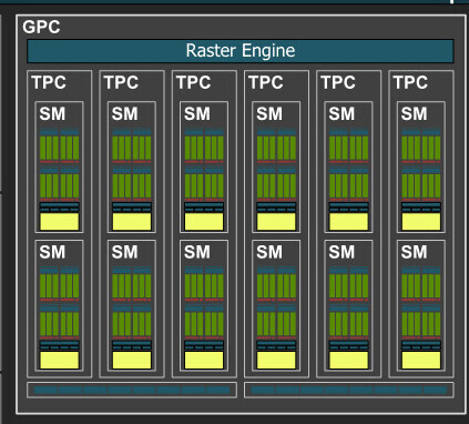
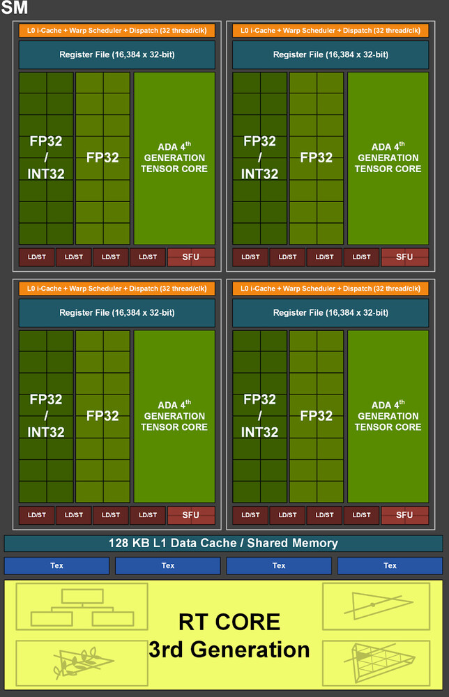
The essential component hierarchy is similar to past generations of NVIDIA GPUs. The AD102 silicon features a whopping 12 Graphics Processing Clusters (GPCs), each of these has all the SIMD and graphics rendering machinery, and is a small GPU in its own right. Each GPC shares a raster engine (geometry processing components) and two ROP partitions (each with eight ROP units). The GPC of the AD102 contains six Texture Processing Clusters (TPCs), the main number-crunching machinery. Each of these has two Streaming Multiprocessors (SM), and a Polymorph unit. Each SM contains 128 CUDA cores across four partitions. Half of these CUDA cores are pure-FP32; while the other half is capable of FP32 or INT32. The SM retains concurrent FP32+INT32 math processing capability. The SM also contains a 3rd generation RT core, four 4th generation Tensor cores, some cache memory, and four TMUs. There are 12 SM per GPC, so 1,536 CUDA cores, 48 Tensor cores, and 12 RT cores; per GPC. Twelve GPCs hence add up to 18,432 CUDA cores, 576 Tensor cores, and 144 RT cores. Each GPC contributes 16 ROPs, so there are a mammoth 192 ROPs on the silicon. A 96 MB L2 cache serves as town-square for the various GPCs, memory controllers, and the PCIe host interface, to exchange data. NVIDIA carved the RTX 4090 out of the AD102 by disabling one of the twelve GPCs, and a further two TPCs from two of the other GPCs, as shown in the red-shaded parts of the block diagram above. The RTX 4090 has 72 MB L2 cache enabled (out of 96 MB physically present on the silicon).


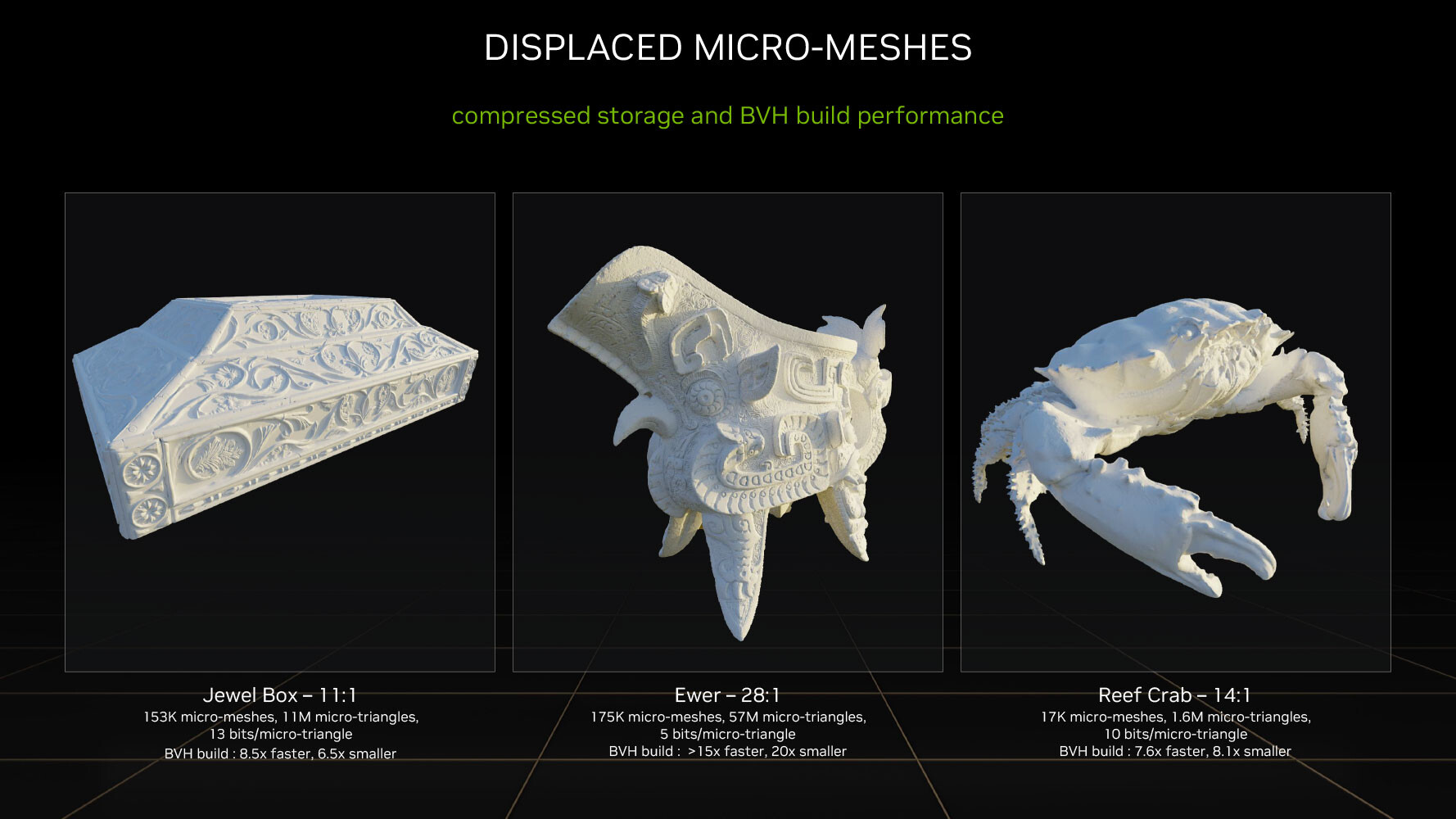
The 3rd generation RT core accelerates the most math-intensive aspects of real-time ray tracing, including BVH traversal. Displaced micro-mesh engine is a revolutionary feature introduced with the new 3rd generation RT core, which accelerates the displaced micro-mesh feature. Just as mesh shaders and tessellation have had a profound impact on improving performance with complex raster geometry, allowing game developers to significantly increase geometric complexity; DMMs is a method to reduce the complexity of the bounding-volume hierarchy (BVH) data-structure, which is used to determine where a ray hits geometry. Previously the BVH had to capture even the smallest details to properly determine the intersection point. Ada's ray tracing architecture receives a major performance uplift from Shader Execution Reordering (SER), a software-defined feature that requires awareness from game-engines, to help the GPU reorganize and optimize worker threads associated with ray tracing.


The BVH now needn't have data for every single triangle on an object, but can represent objects with complex geometry as a coarse mesh of base triangles, which greatly simplifies the BVH data structure. A simpler BVH means less memory consumed and helps to greatly reduce ray tracing CPU load, because the CPU only has to generate a smaller structure. With older "Ampere" and "Turing" RT cores, each triangle on an object had to be sampled at high overhead, so the RT core could precisely calculate ray intersection for each triangle. With Ada, the simpler BVH, plus the displacement maps can be sent to the RT core, which is now able to figure out the exact hit point on its own. NVIDIA has seen 11:1 to 28:1 compression in total triangle counts. This reduces BVH compile times by 7.6x to over 15x, in comparison to the older RT core; and reducing its storage footprint by anywhere between 6.5 to 20 times. DMMs could reduce disk- and memory bandwidth utilization, utilization of the PCIe bus, as well as reduce CPU utilization. NVIDIA worked with Simplygon and Adobe to add DMM support for their tool chains.

Opacity Micro Meshes (OMM) is a new feature introduced with Ada to improve rasterization performance, particularly with objects that have alpha (transparency data). Most low-priority objects in a 3D scene, such as leaves on a tree, are essentially rectangles with textures on the leaves where the transparency (alpha) creates the shape of the leaf. RT cores have a hard time intersecting rays with such objects, because they're not really in the shape that they appear (they're really just rectangles with textures that give you the illusion of shape). Previous-generation RT cores had to have multiple interactions with the rendering stage to figure out the shape of a transparent object, because they couldn't test for alpha by themselves.
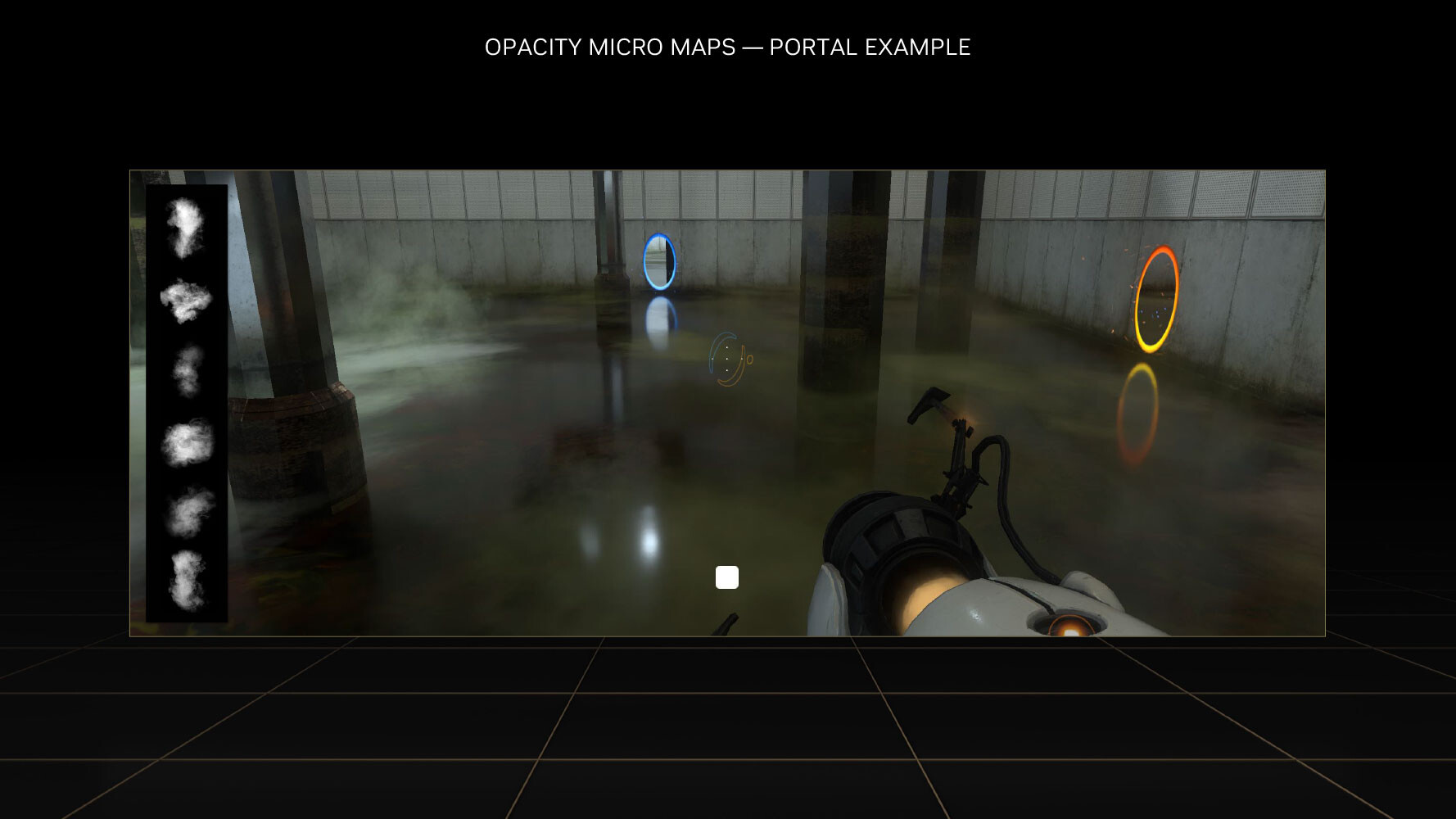

This has been solved by using OMMs. Just as DMMs simplify geometry by creating meshes of micro-triangles; OMMs create meshes of rectangular textures that align with parts of the texture that aren't alpha, so the RT core has a better understanding of the geometry of the object, and can correctly calculate ray intersections. This has a significant performance impact on shading performance in non-RT applications, too. Practical applications of OMMs aren't just low-priority objects such as vegetation, but also smoke-sprites and localized fog. Traditionally there was a lot of overdraw for such effects, because they layered multiple textures on top of each other, that all had to be fully processed by the shaders. Now only the non-opaque pixels get executed—OMMs provide a 30 percent speedup with graphics buffer fill-rates, and a 10 percent impact on frame-rates.

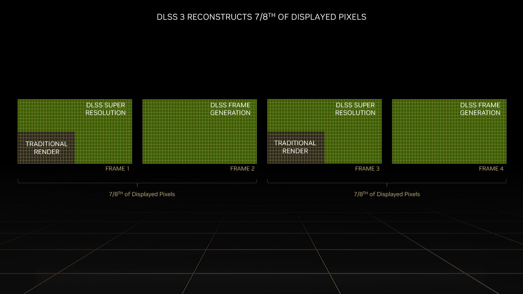
DLSS 3 introduces a revolutionary new feature that promises a doubling in frame-rate at comparable quality, it's called AI frame-generation. While it has all the features of DLSS 2 and its AI super-resolution (scaling up a lower-resolution frame to native resolution with minimal quality loss); DLSS 3 can generate entire frames simply using AI, without involving the graphics rendering pipeline.

Every alternating frame with DLSS 3 is hence AI-generated, without being a replica of the previous rendered frame. This is possible only on the Ada graphics architecture, because of a hardware component called the optical flow accelerator (OFA), which assists in predicting what the next frame could look like, by creating what NVIDIA calls an optical flow-field. OFA ensures that the DLSS 3 algorithm isn't confused by static objects in a rapidly-changing 3D scene (such as a race sim). The process heavily relies on the performance uplift introduced by the FP8 math format of the 4th generation Tensor core. A third key ingredient of DLSS 3 is Reflex. By reducing the rendering queue to zero, Reflex plays a vital role in ensuring that frame-times with DLSS 3 are at an acceptable level, and a render-queue doesn't confuse the upscaler. A combination of OFA and the 4th Gen Tensor core is why the Ada architecture is required to use DLSS 3, and why it won't work on older architectures.
Packaging
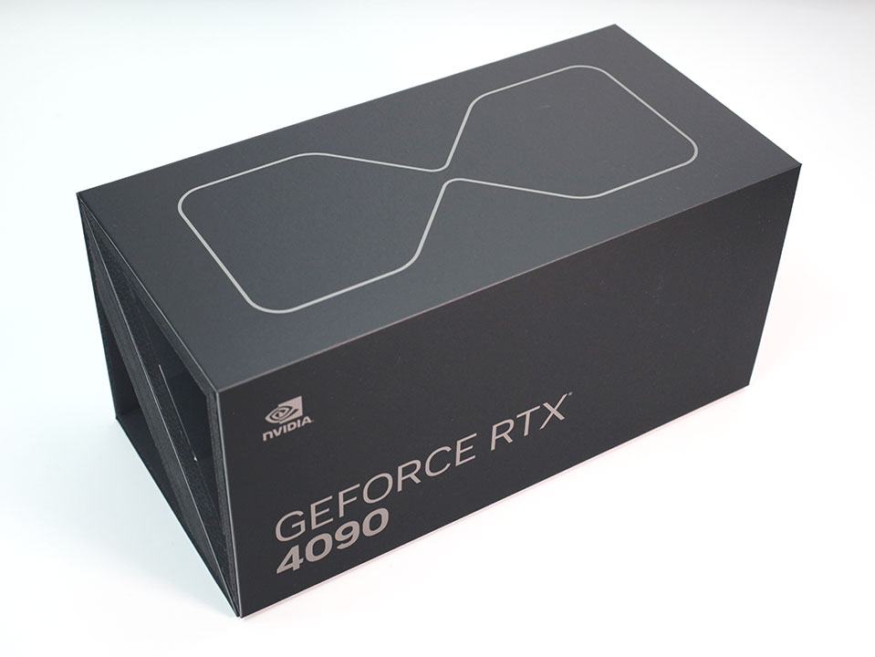

RTX 4090 Founders Edition comes in a huge flip-open package.

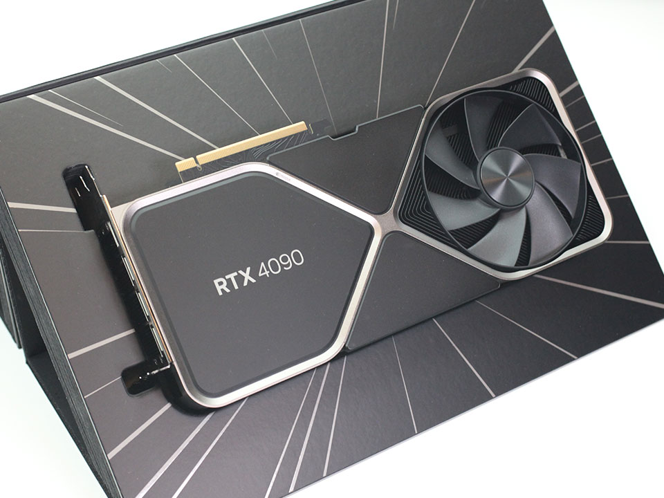
The card sits neatly in the center, underneath the card you'll find documentation and the PCIe adapter cable.
The Card


NVIDIA's Founders Edition looks stunning—it could be an Apple product. NVIDIA has made small improvements to the design language, making it an even cleaner design than what we saw on GeForce 30 Series. As with Ampere, the card is designed for airflow to go through the card—that's why there's two fans. One sucks in cool air from the bottom, is pushed through the card and then blown out towards the case top on the other side.

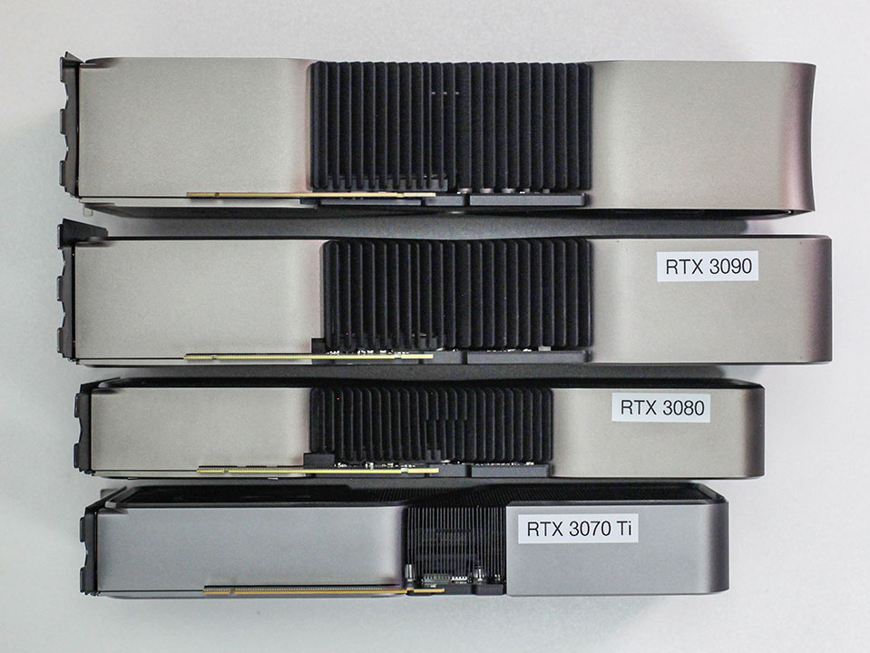
Comparison against the GeForce 30 Series.
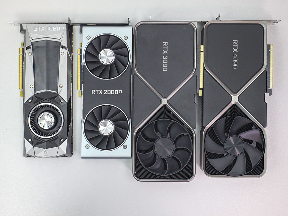
From left to right: GTX 1080 Ti, RTX 2080 Ti, RTX 3090, RTX 4090.
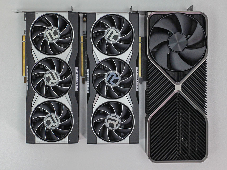

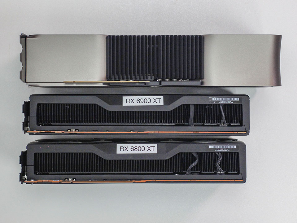
Compared against AMD's recent offerings it becomes clear how large this card really is.
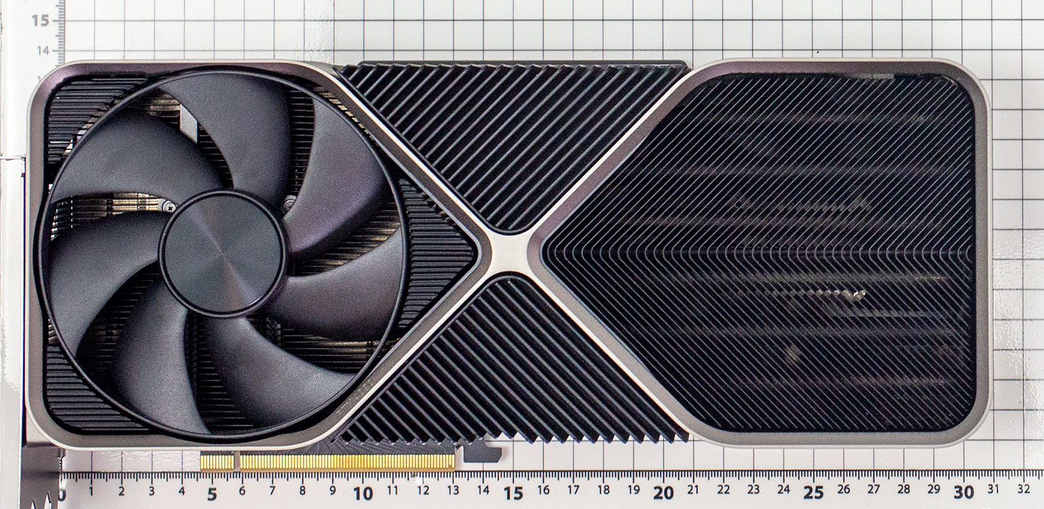

Dimensions of the card are 31.0 x 14.0 cm, and it weighs 2181 g.


Installation requires three slots in your system.

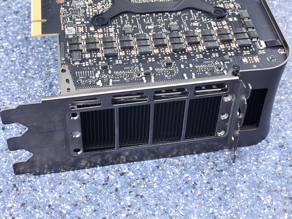
Display connectivity includes three standard DisplayPort 1.4a ports and one HDMI 2.1a (same as Ampere).
NVIDIA introduces the concept of dual NVDEC and NVENC Codecs with the Ada architecture. This means there are now two independent sets of hardware-accelerators; so you can encode and decode two streams of video in parallel, or one stream at double the FPS rate. The new 8th Gen NVENC now accelerates AV1 encoding, besides HEVC. You also get an "optical flow accelerator" unit that is able to calculate intermediate frames for videos, to smooth playback. The same hardware unit is used for frame generation in DLSS 3.
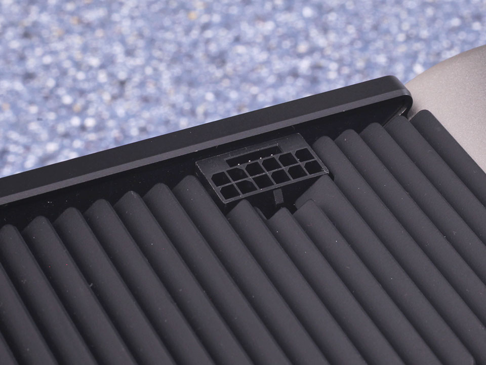

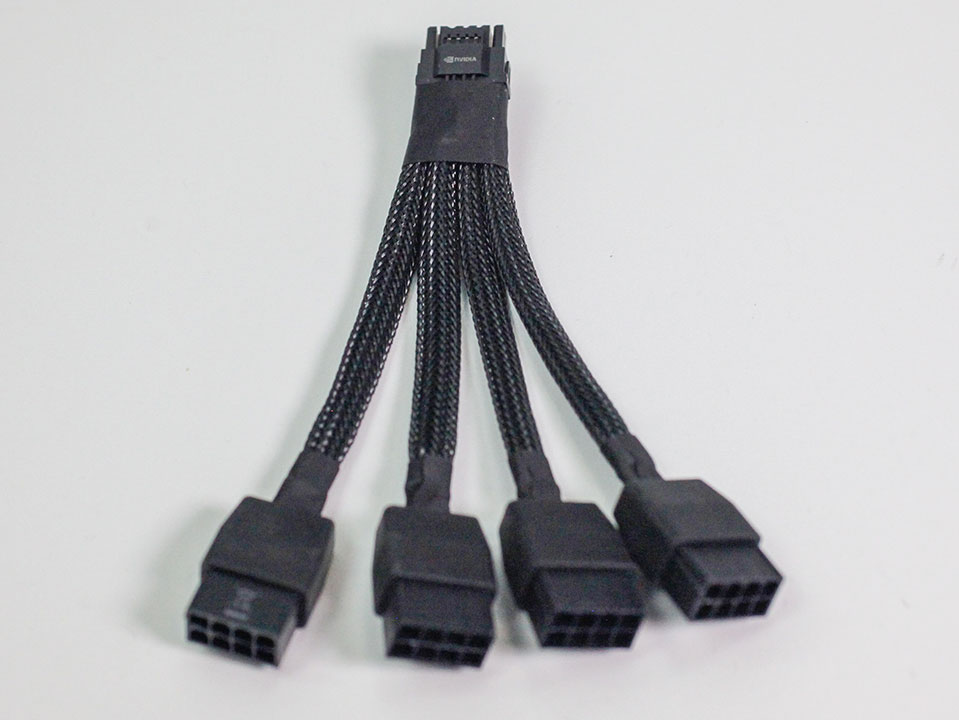
The card uses the new 12+4 pin ATX 12VHPWR connector, which is rated for up to 600 W of power draw. An adapter cable from 4x PCIe 8-pin is included, you can also run the card with just three 8-pins. The default power limit is 450 W, so it'll be perfectly fine and within spec (even with one 8-pin left unconnected). At the top of the 16-pin connector there's four "sense" pins, which signal to the graphics card how many power cables are connected, so the card can adjust power limits automatically.

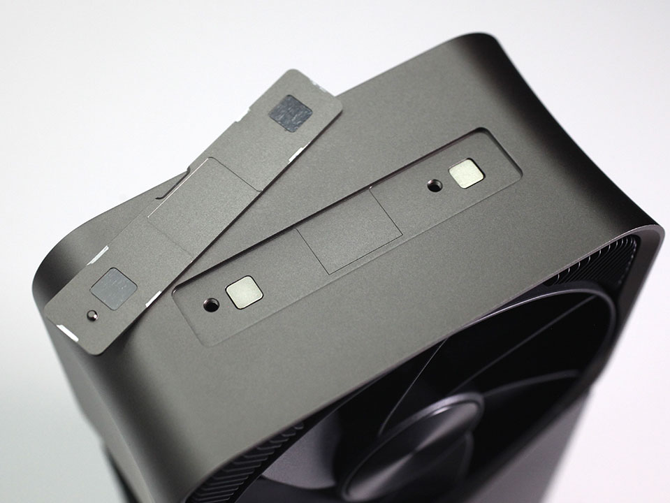
The tail end of the card has a small lid that covers the mounting holes for a support rail, used in certain workstation form-factors such as the x86 Mac Pro.
Teardown
Taking the RTX 4090 Founders Edition apart isn't much different to previous Founders Edition cards and can be done in a few minutes, if you know what you're doing.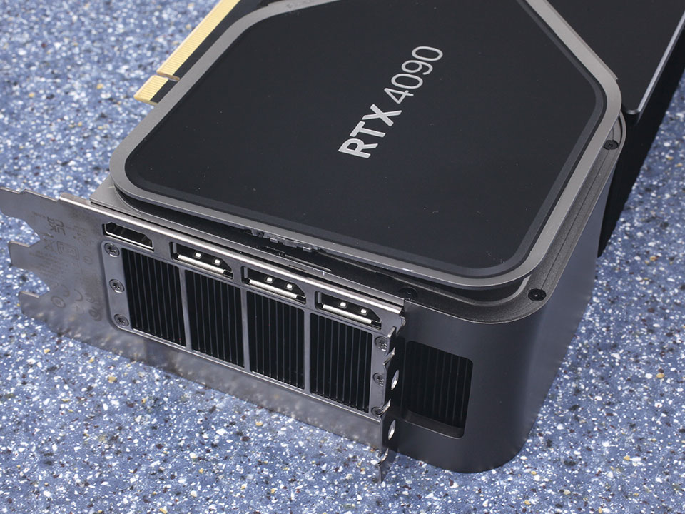
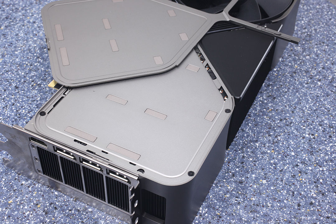
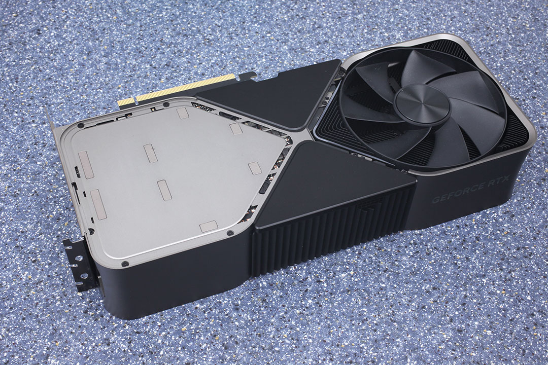
First pop off the top cover with the "RTX 4090" text on it. To do that carefully lift it up from the PCIe slot cover side, it's attached magnetically.


The metal plate is a really nice design, I love the idea with the magnets. Everything stays in place during normal use, yet it's easy to disassemble the RTX 4090—and no glue is used.
Next, remove four Philips screws and four Torx screws.
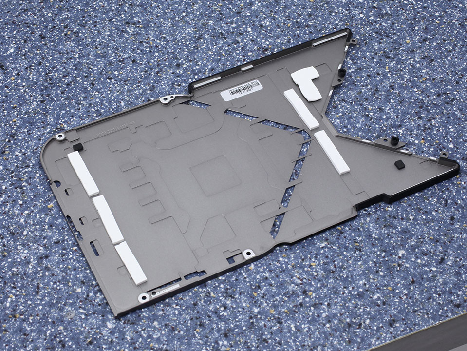
This is like the classic "backplate", it has a few thermal pads to soak up (a little bit of) heat from the card underneath.
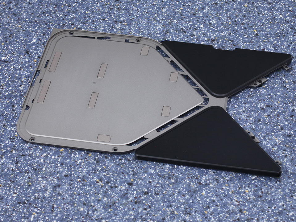
Now you can remove the six Torx screws on the slot cover, and one more screw near the top right in the 2nd picture, that holds the slot cover in place.
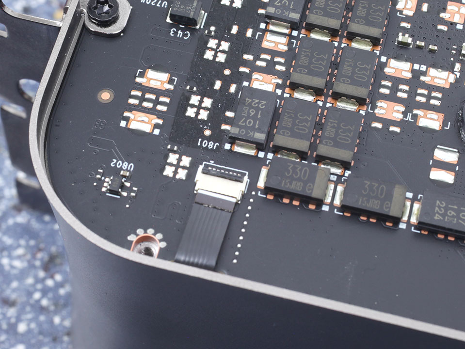


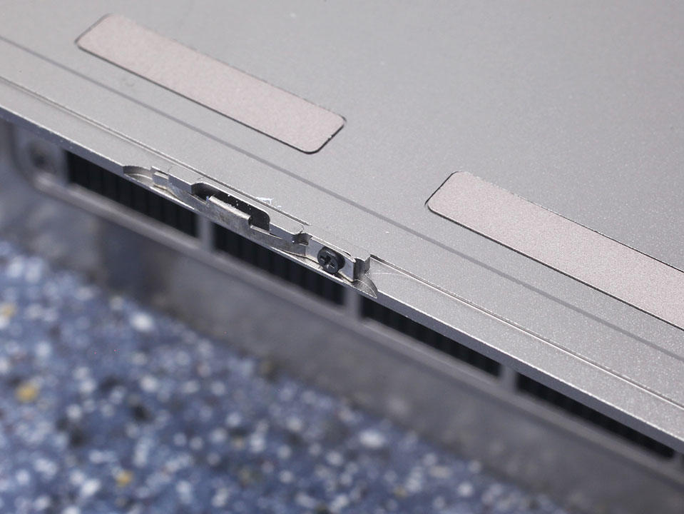
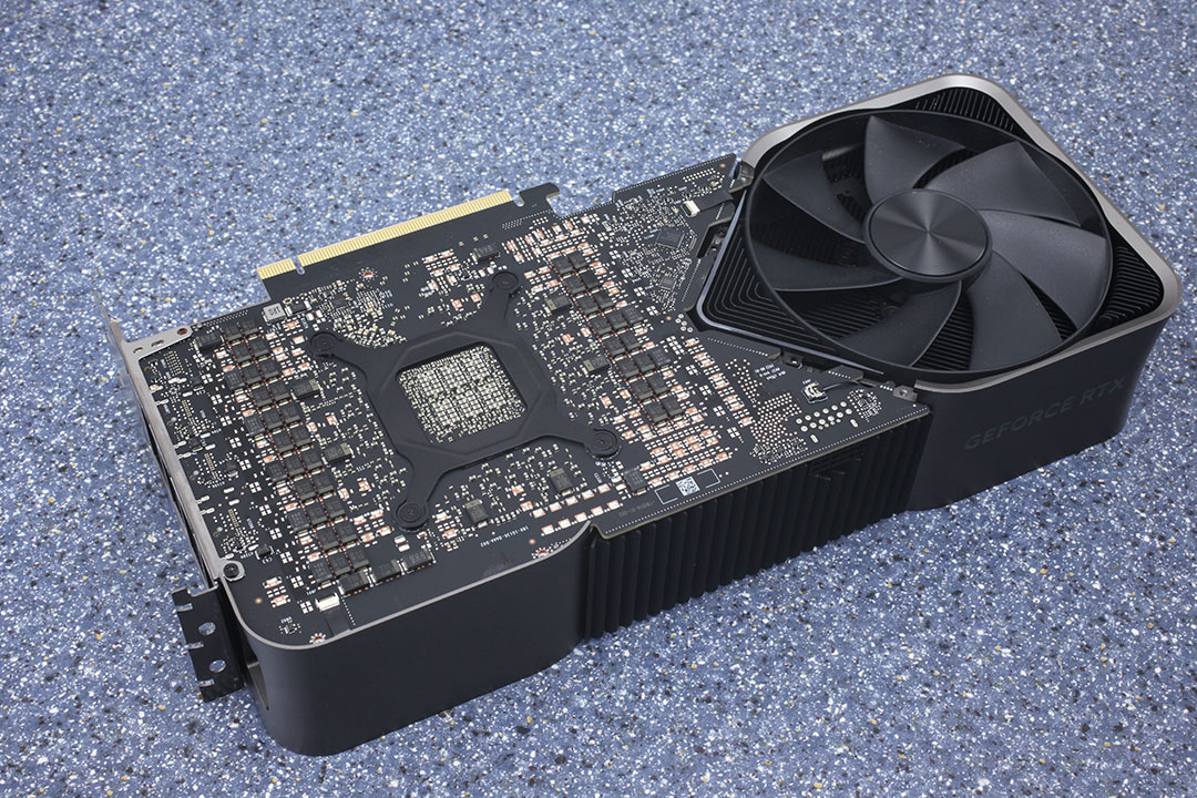
We've seen these before, flip up the flat-ribbon connector carefully (I prefer to use my fingers rather than pliers), and carefully pull out the flat-ribbon cable. The other connector, with the silvery cover requires you to push the cover sideways and then you can lift the black plastic connector upwards. More info here.

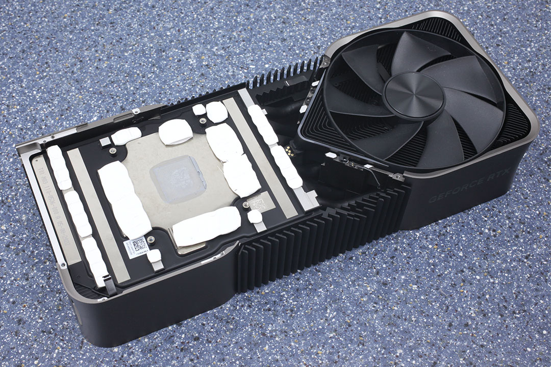
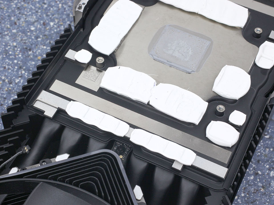
This is a beast of a cooler—there's tons of thermal pads to provide cooling not only for the GPU, but also the VRM and memory chips.

Please note how NVIDIA cut grooves into the heatsink for the memory pads—it's the first time that I see such an approach. I think it will definitely help improve contact, especially in situations where the thermal pad might be somewhat too thin or the mounting is slightly suboptimal.
NVIDIA uses six fat heatpipes and a vapor-chamber plate to move heat away from the GPU quickly.
High-resolution PCB Pictures
These pictures are for the convenience of volt modders and people who would like to see all the finer details on the PCB. Feel free to link back to us and use these in your articles, videos or forum posts.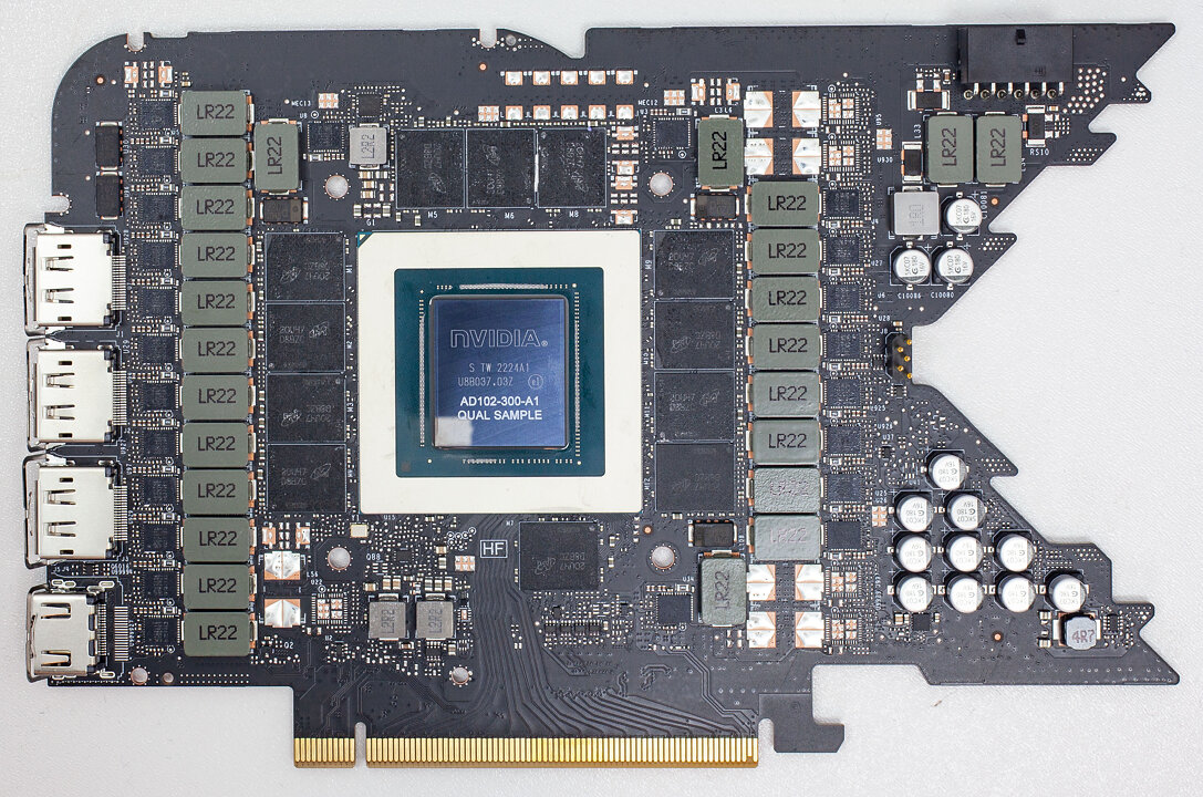
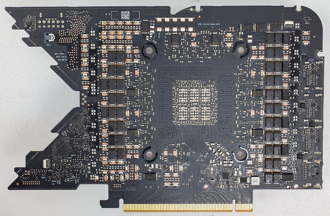
High-resolution versions are also available (front, back).
Our Patreon Silver Supporters can read articles in single-page format.
May 16th, 2024 08:01 EDT
change timezone
Latest GPU Drivers
New Forum Posts
- Would you pay more for hardware with AI capabilities? (22)
- Double radiator setup with GPU fans on top (7)
- EULA in Games (18)
- AIO Water Cooler vs Tower Air Cooler (23)
- Post Your TIMESPY, PCMARK10 & FIRESTRIKE SCORES! (2019) (220)
- Ads in forums. under news (10)
- Ubuntu 24.04 LTS released (31)
- Homeworld 3 [Official Thread] (42)
- What's your latest tech purchase? (20533)
- Unknown Subvendor in GPU-Z (2)
Popular Reviews
- Homeworld 3 Performance Benchmark Review - 35 GPUs Tested
- Enermax REVOLUTION D.F. X 1200 W Review
- Lofree Edge Ultra-Low Profile Wireless Mechanical Keyboard Review
- Upcoming Hardware Launches 2023 (Updated Feb 2024)
- ZMF Caldera Closed Planar Magnetic Headphones Review
- AMD Ryzen 7 7800X3D Review - The Best Gaming CPU
- Corsair MP700 Pro SE 4 TB Review
- ASUS Radeon RX 7900 GRE TUF OC Review
- ThundeRobot ML903 NearLink Review
- Sapphire Radeon RX 7900 GRE Pulse Review
Controversial News Posts
- Intel Statement on Stability Issues: "Motherboard Makers to Blame" (267)
- AMD to Redesign Ray Tracing Hardware on RDNA 4 (227)
- Windows 11 Now Officially Adware as Microsoft Embeds Ads in the Start Menu (172)
- NVIDIA to Only Launch the Flagship GeForce RTX 5090 in 2024, Rest of the Series in 2025 (152)
- AMD Hits Highest-Ever x86 CPU Market Share in Q1 2024 Across Desktop and Server (137)
- AMD RDNA 5 a "Clean Sheet" Graphics Architecture, RDNA 4 Merely Corrects a Bug Over RDNA 3 (127)
- AMD's RDNA 4 GPUs Could Stick with 18 Gbps GDDR6 Memory (114)
- AMD Ryzen 9 7900X3D Now at a Mouth-watering $329 (104)