 5
5
Palit GeForce RTX 4070 JetStream Review
(5 Comments) »Introduction
Palit GeForce RTX 4070 JetStream is a premium custom-design graphics card based on the newest kid on the block, the RTX 4070 Ada, a performance-segment ace by NVIDIA designed for maxed out AAA gaming at 1440p, including ray tracing. The new features introduced with Ada, such as multiple video encoding streams, and of course DLSS 3 Frame Generation, are expected to position the RTX 4070 as a superior proposition to the deluge of previous-generation graphics cards being sold around this price these days, to clear inventory, not to mention superior energy efficiency from the chip's 5 nm process node.

The GeForce RTX 4070 is designed for not just maxed out 1440p gaming, but also high refresh-rate e-sports gaming. 4K Ultra HD is within its reach, if you know your way around game settings, or rely on GeForce Experience to find you the best ones. You can also use DLSS and Frame Generation to your advantage. The GeForce Ada graphics architecture debuts the 3rd generation of NVIDIA RTX real time ray tracing technology, faster and more capable CUDA cores that operate at higher frequencies; 3rd generation RT cores with even more hardware-accelerated capabilities, and 4th generation Tensor cores with support for even more math formats. The Optical Flow Accelerator component enables DLSS 3, a feature that generates entire alternate frames entirely using AI, without involving much of the graphics rendering machinery.
The GeForce RTX 4070 we're reviewing today is based on the same 5 nm AD104 GPU as the RTX 4070 Ti, but while the latter maxes out the silicon, the RTX 4070 is heavily cut down from it. This GPU is endowed with 5,888 CUDA cores, 46 RT cores, 184 Tensor cores, 64 ROPs, and 184 TMUs. It gets these many shaders by enabling 46 out of the 60 streaming multiprocessors (SM) present on the silicon. The memory configuration is unchanged from the RTX 4070 Ti—you still get 12 GB of 21 Gbps GDDR6X memory across a 192-bit wide memory bus, with 504 GB/s of bandwidth on tap. The bandwidth is higher than the 448 GB/s that the previous-generation RTX 3070 contends with. The 192-bit memory bus may seem narrow, but is the result of NVIDIA trying to restructure the memory sub-system, with greater use of on-die caches on the GPU.
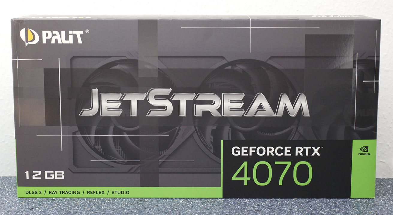
The JetStream brand from Palit represented the company's very best in custom-design for quiet and capable gaming PC builds, until the SKU got topped by the Palit GameRock and GamingPro series. The RTX 4070 JetStream features a meaty triple-slot, triple-fan cooler. There's no RGB lighting on offer, but you're promised low gaming noise from the larger cooler. The card ticks at NVIDIA-reference clock speeds of up to 2475 MHz GPU Boost. Palit also opted for the more familiar and convenient 8-pin PCIe power connector in place of the 12VHPWR connector, which should do just fine, given the 200 W TGP for the RTX 4070. While Palit hasn't given us an exact price point, they only confirmed that its price "will be a little higher than $599." Throughout this review we've assumed a $620 price.
| Price | Cores | ROPs | Core Clock | Boost Clock | Memory Clock | GPU | Transistors | Memory | |
|---|---|---|---|---|---|---|---|---|---|
| Arc A770 | $290 | 4096 | 128 | 2100 MHz | N/A | 2187 MHz | ACM-G10 | 21700M | 16 GB, GDDR6, 256-bit |
| RTX 2080 | $310 | 2944 | 64 | 1515 MHz | 1710 MHz | 1750 MHz | TU104 | 13600M | 8 GB, GDDR6, 256-bit |
| RTX 3060 Ti | $320 | 4864 | 80 | 1410 MHz | 1665 MHz | 1750 MHz | GA104 | 17400M | 8 GB, GDDR6, 256-bit |
| RX 6700 XT | $320 | 2560 | 64 | 2424 MHz | 2581 MHz | 2000 MHz | Navi 22 | 17200M | 12 GB, GDDR6, 192-bit |
| RTX 2080 Ti | $420 | 4352 | 88 | 1350 MHz | 1545 MHz | 1750 MHz | TU102 | 18600M | 11 GB, GDDR6, 352-bit |
| RTX 3070 | $400 | 5888 | 96 | 1500 MHz | 1725 MHz | 1750 MHz | GA104 | 17400M | 8 GB, GDDR6, 256-bit |
| RTX 3070 Ti | $500 | 6144 | 96 | 1575 MHz | 1770 MHz | 1188 MHz | GA104 | 17400M | 8 GB, GDDR6X, 256-bit |
| RX 6800 | $450 | 3840 | 96 | 1815 MHz | 2105 MHz | 2000 MHz | Navi 21 | 26800M | 16 GB, GDDR6, 256-bit |
| RX 6800 XT | $510 | 4608 | 128 | 2015 MHz | 2250 MHz | 2000 MHz | Navi 21 | 26800M | 16 GB, GDDR6, 256-bit |
| RTX 3080 | $550 | 8704 | 96 | 1440 MHz | 1710 MHz | 1188 MHz | GA102 | 28000M | 10 GB, GDDR6X, 320-bit |
| RTX 4070 | $600 | 5888 | 64 | 1920 MHz | 2475 MHz | 1313 MHz | AD104 | 35800M | 12 GB, GDDR6X, 192-bit |
| Palit RTX 4070 JetStream | $620 | 5888 | 64 | 1920 MHz | 2475 MHz | 1313 MHz | AD104 | 35800M | 12 GB, GDDR6X, 192-bit |
| RTX 3080 Ti | $750 | 10240 | 112 | 1365 MHz | 1665 MHz | 1188 MHz | GA102 | 28000M | 12 GB, GDDR6X, 384-bit |
| RX 6900 XT | $620 | 5120 | 128 | 2015 MHz | 2250 MHz | 2000 MHz | Navi 21 | 26800M | 16 GB, GDDR6, 256-bit |
| RX 6950 XT | $680 | 5120 | 128 | 2100 MHz | 2310 MHz | 2250 MHz | Navi 21 | 26800M | 16 GB, GDDR6, 256-bit |
| RTX 3090 | $800 | 10496 | 112 | 1395 MHz | 1695 MHz | 1219 MHz | GA102 | 28000M | 24 GB, GDDR6X, 384-bit |
| RTX 4070 Ti | $800 | 7680 | 80 | 2310 MHz | 2610 MHz | 1313 MHz | AD104 | 35800M | 12 GB, GDDR6X, 192-bit |
| RX 7900 XT | $800 | 5376 | 192 | 2000 MHz | 2400 MHz | 2500 MHz | Navi 31 | 57700M | 20 GB, GDDR6, 320-bit |
| RTX 3090 Ti | $1000 | 10752 | 112 | 1560 MHz | 1950 MHz | 1313 MHz | GA102 | 28000M | 24 GB, GDDR6X, 384-bit |
| RTX 4080 | $1150 | 9728 | 112 | 2205 MHz | 2505 MHz | 1400 MHz | AD103 | 45900M | 16 GB, GDDR6X, 256-bit |
| RX 7900 XTX | $960 | 6144 | 192 | 2300 MHz | 2500 MHz | 2500 MHz | Navi 31 | 57700M | 24 GB, GDDR6, 384-bit |
| RTX 4090 | $1600 | 16384 | 176 | 2235 MHz | 2520 MHz | 1313 MHz | AD102 | 76300M | 24 GB, GDDR6X, 384-bit |
Architecture
The Ada graphics architecture heralds the third generation of the NVIDIA RTX technology, an effort toward increasing the realism of game visuals by leveraging real-time ray tracing, without the enormous amount of compute power required to draw purely ray-traced 3D graphics. This is done by blending conventional raster graphics with ray traced elements such as reflections, lighting, and global illumination, to name a few. The 3rd generation of RTX introduces the new higher IPC "Ada" CUDA core, 3rd generation RT core, 4th generation Tensor core, and the new Optical Flow Processor, a component that plays a key role in generating new frames without involving the GPU's main graphics rendering pipeline.


The GeForce Ada graphics architecture driving the RTX 4070 leverages the TSMC 5 nm EUV foundry process to increase transistor counts. At the heart of this GPU is the new AD104 silicon, which has a fairly high transistor count of 35.8 billion, which is more than double that of the previous-generation GA104. The GPU features a PCI-Express 4.0 x16 host interface, and a 192-bit wide GDDR6X memory bus, which on the RTX 4070 wires out to 12 GB of memory. The Optical Flow Accelerator (OFA) is an independent top-level component. The chip features one NVENC and one NVDEC unit.
The essential component hierarchy is similar to past generations of NVIDIA GPUs. The AD104 silicon features 5 Graphics Processing Clusters (GPCs), each of these has all the SIMD and graphics rendering machinery, and is a small GPU in its own right. Each GPC shares a raster engine (geometry processing components) and two ROP partitions (each with eight ROP units). The GPC of the AD104 contains six Texture Processing Clusters (TPCs), the main number-crunching machinery. Each of these has two Streaming Multiprocessors (SM), and a Polymorph unit. Each SM contains 128 CUDA cores across four partitions. Half of these CUDA cores are pure-FP32; while the other half is capable of FP32 or INT32. The SM retains concurrent FP32+INT32 math processing capability. The SM also contains a 3rd generation RT core, four 4th generation Tensor cores, some cache memory, and four TMUs. There are 12 SM per GPC, so 1,536 CUDA cores, 48 Tensor cores, and 12 RT cores; per GPC. There are five such GPCs, which add up to 7,680 CUDA cores, 240 TMUs, 240 Tensor Cores, and 60 RT cores. Each GPC contributes 16 ROPs, so there are 80 ROPs on the silicon. The RTX 4070 is carved out of the AD104 by disabling an entire GPC worth 6 TPCs, and an additional TPC from one of the remaining GPCs. This yields 5,888 CUDA cores, 184 Tensor cores, 46 RT cores, and 184 TMUs. The ROP count has been reduced from 80 to 64. The on-die L2 cache sees a slight reduction, too, which is now down to 36 MB from the 48 MB present.


The 3rd generation RT core accelerates the most math-intensive aspects of real-time ray tracing, including BVH traversal. Displaced micro-mesh engine is a revolutionary feature introduced with the new 3rd generation RT core. Just as mesh shaders and tessellation have had a profound impact on improving performance with complex raster geometry, allowing game developers to significantly increase geometric complexity; DMM is a method to reduce the complexity of the bounding-volume hierarchy (BVH) data-structure, which is used to determine where a ray hits geometry. Previously, the BVH had to capture even the smallest details to properly determine the intersection point. Ada's ray tracing architecture also receives a major performance uplift from Shader Execution Reordering (SER), a software-defined feature that requires awareness from game-engines, to help the GPU reorganize and optimize worker threads associated with ray tracing.


The BVH now needn't have data for every single triangle on an object, but can represent objects with complex geometry as a coarse mesh of base triangles, which greatly simplifies the BVH data structure. A simpler BVH means less memory consumed and helps to greatly reduce ray tracing CPU load, because the CPU only has to generate a smaller structure. With older "Ampere" and "Turing" RT cores, each triangle on an object had to be sampled at high overhead, so the RT core could precisely calculate ray intersection for each triangle. With Ada, the simpler BVH, plus the displacement maps can be sent to the RT core, which is now able to figure out the exact hit point on its own. NVIDIA has seen 11:1 to 28:1 compression in total triangle counts. This reduces BVH compile times by 7.6x to over 15x, in comparison to the older RT core; and reducing its storage footprint by anywhere between 6.5 to 20 times. DMM could reduce disk- and memory bandwidth utilization, utilization of the PCIe bus, as well as reduce CPU utilization. NVIDIA worked with Simplygon and Adobe to add DMM support for their tool chains.


Opacity Micro Meshes (OMM) is a new feature introduced with Ada to improve rasterization performance, particularly with objects that have alpha (transparency data). Most low-priority objects in a 3D scene, such as leaves on a tree, are essentially rectangles with textures on the leaves where the transparency (alpha) creates the shape of the leaf. RT cores have a hard time intersecting rays with such objects, because they're not really in the shape that they appear (they're really just rectangles with textures that give you the illusion of shape). Previous-generation RT cores had to have multiple interactions with the rendering stage to figure out the shape of a transparent object, because they couldn't test for alpha by themselves.


This has been solved by using OMMs. Just as DMMs simplify geometry by creating meshes of micro-triangles; OMMs create meshes of rectangular textures that align with parts of the texture that aren't alpha, so the RT core has a better understanding of the geometry of the object, and can correctly calculate ray intersections. This has a significant performance impact on shading performance in non-RT applications, too. Practical applications of OMMs aren't just low-priority objects such as vegetation, but also smoke-sprites and localized fog. Traditionally there was a lot of overdraw for such effects, because they layered multiple textures on top of each other, that all had to be fully processed by the shaders. Now only the non-opaque pixels get executed—OMMs provide a 30 percent speedup with graphics buffer fill-rates, and a 10 percent impact on frame-rates.


DLSS 3 introduces a revolutionary new feature that promises a doubling in frame-rate at comparable quality, it's called AI frame-generation. While it has all the features of DLSS 2 and its AI super-resolution (scaling up a lower-resolution frame to native resolution with minimal quality loss); DLSS 3 can generate entire frames simply using AI, without involving the graphics rendering pipeline. Later in the article, we will show you DLSS 3 in action.


Every alternating frame with DLSS 3 is hence AI-generated, without being a replica of the previous rendered frame. This is possible only on the Ada graphics architecture, because of a hardware component called the optical flow accelerator (OFA), which assists in predicting what the next frame could look like, by creating what NVIDIA calls an optical flow-field. OFA ensures that the DLSS 3 algorithm isn't confused by static objects in a rapidly-changing 3D scene (such as a race sim). The process heavily relies on the performance uplift introduced by the FP8 math format of the 4th generation Tensor core. A third key ingredient of DLSS 3 is Reflex. By reducing the rendering queue to zero, Reflex plays a vital role in ensuring that frame-times with DLSS 3 are at an acceptable level, and a render-queue doesn't confuse the upscaler. A combination of OFA and the 4th Gen Tensor core is why the Ada architecture is required to use DLSS 3, and why it won't work on older architectures.
Packaging
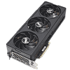
The Card


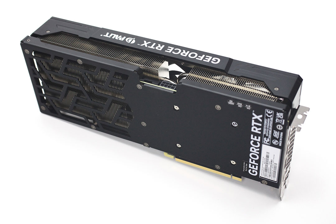
Palit's RTX 4070 JetStream uses a mostly black color theme, which looks good, thanks to the matte surfaces. On the other side you'll find a metal backplate that has a cutout for air to flow through.

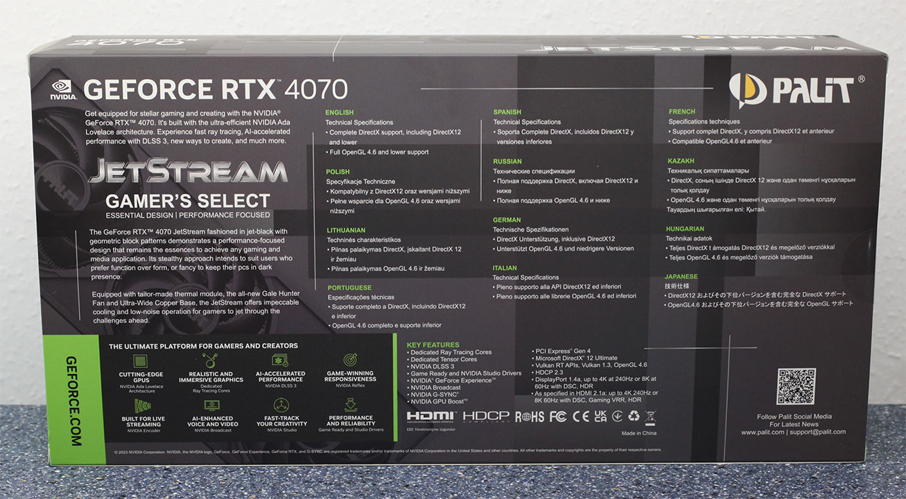
Dimensions of the card are 33 x 13 cm, and it weighs 1455 g.
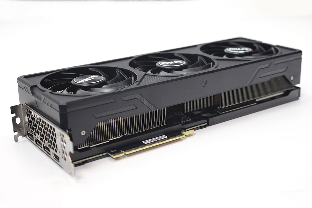
Installation requires three slots in your system.

Display connectivity includes three standard DisplayPort 1.4a ports and one HDMI 2.1a (same as Ampere).
The new 8th Gen NVENC now accelerates AV1 encoding, besides HEVC. You also get an "optical flow accelerator" unit that is able to calculate intermediate frames for videos, to smooth playback. The same hardware unit is used for frame generation in DLSS 3.
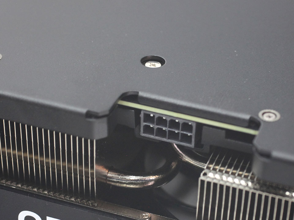
The card uses a single 8-pin power connector, which, together with the PCIe slot, is specified for up to 225 W power draw. Some other RTX 4070 cards like the NVIDIA Founders Edition come with the new 16-pin connector, but they are limited to the same power draw levels. NVIDIA has given their partners free choice on what connector they use, and I suspect the classic 8-pin is a little bit cheaper to implement.
Teardown
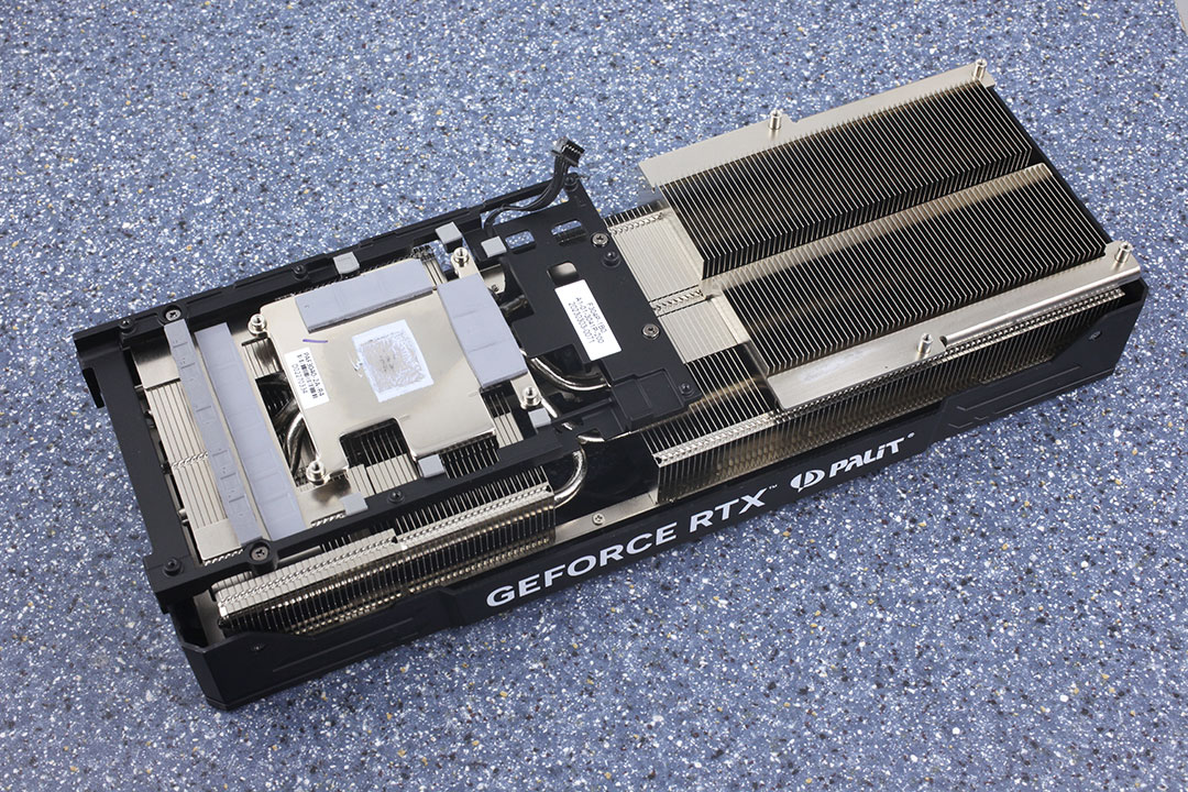

Palit's heatsink uses six heatpipes to keep the card cool. The main cooler also provides cooling for the memory chips and VRM circuitry.

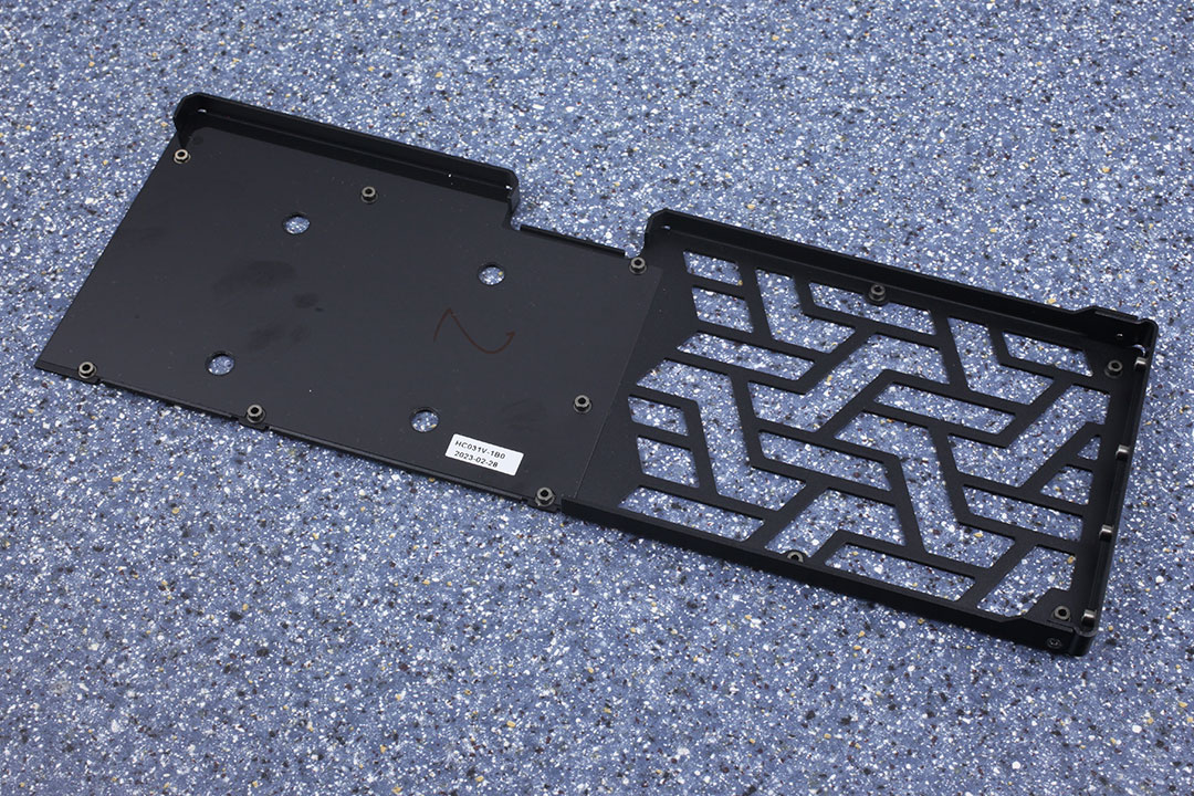
The metal backplate protects the card against damage during installation and handling.
High-resolution PCB Pictures
These pictures are for the convenience of volt modders and people who would like to see all the finer details on the PCB. Feel free to link back to us and use these in your articles, videos or forum posts.

High-resolution versions are also available (front, back).
Circuit Board (PCB) Analysis


GPU voltage is a six-phase design, managed by a uPI uP9512R controller.

OnSemi NCP302150 DrMOS components are used for GPU voltage; they are rated for 50 A of current each.


Memory voltage is a two-phase design, managed by a uPI uP9529Q controller.

For memory, OnSemi NCP302150 DrMOS with a 50 A rating are used again.

The GDDR6X memory chips are made by Micron and carry the model number D8BZC, which decodes to MT61K512M32KPA-21:U. They are specified to run at 1313 MHz (21 Gbps GDDR6 effective).

NVIDIA's AD104 graphics processor is the company's third Ada Lovelace GPU. It is built using a 5 nanometer process at TSMC Taiwan, with a transistor count of 35.8 billion and a die size of 295 mm².
Our Patreon Silver Supporters can read articles in single-page format.
Jun 4th, 2024 22:45 EDT
change timezone
Latest GPU Drivers
New Forum Posts
- Insyde software announces AI BIOS! (8)
- What's your latest tech purchase? (20734)
- Zen5 only 16 core. (43)
- 3DMARK "LEGENDARY" (224)
- Star Wars: Outlaws - Let's be honest, who's gonna pre-order on UbiSoft? (38)
- Dell Workstation Owners Club (3104)
- Windows 7 and Gigabyte 299x wu8 (13)
- All Intel DG1 needs special bios? (27)
- Post your cooling. (61)
- Have you got pie today? (16358)
Popular Reviews
- Intel Lunar Lake Technical Deep Dive - So many Revolutions in One Chip
- Kioxia Exceria Plus G3 2 TB Review
- Corsair iCUE XC7 RGB Elite LCD CPU Water Block Review
- NZXT H6 Flow RGB Review
- SilverStone KL07E Review
- Upcoming Hardware Launches 2024 (Updated May 2024)
- NuPhy Air96 V2 Low Profile Wireless Mechanical Keyboard Review
- AMD Ryzen 7 7800X3D Review - The Best Gaming CPU
- Ghost of Tsushima Performance Benchmark Review - 35 GPUs Tested
- ASUS GeForce RTX 4060 Dual OC Review - The Best RTX 4060
Controversial News Posts
- NVIDIA to Only Launch the Flagship GeForce RTX 5090 in 2024, Rest of the Series in 2025 (154)
- AMD Hits Highest-Ever x86 CPU Market Share in Q1 2024 Across Desktop and Server (140)
- AMD RDNA 5 a "Clean Sheet" Graphics Architecture, RDNA 4 Merely Corrects a Bug Over RDNA 3 (139)
- NVIDIA RTX 5090 "Blackwell" Founders Edition to Implement the "RTX 4090 Ti" Cinderblock Design (118)
- Core Configurations of Intel Core Ultra 200 "Arrow Lake-S" Desktop Processors Surface (101)
- Biden Administration to Revive Trump-Era Tariffs on China-made GPUs and Motherboards (95)
- AMD Ryzen 9000 Zen 5 Single Thread Performance at 5.80 GHz Found 19% Over Zen 4 (88)
- ASRock Innovates First AMD Radeon RX 7000 Graphics Card with 12V-2x6 Power Connector (88)