 6
6
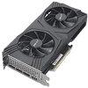
PNY GeForce RTX 4070 Super Verto Review
(6 Comments) »Introduction
NVIDIA today launched the new GeForce RTX 4070 SUPER, and allowed us to share with you how cards priced at its MSRP perform, custom OC cards can be reviewed tomorrow. For this review, we have with us the PNY RTX 4070 SUPER Verto. If you're in the market for a particular GPU and don't care about the 1-3% performance difference that the more expensive overclocked cards command, you'd want to look for cards priced at the baseline. They are designed to meet the performance outlook of the GPU at a price NVIDIA is quoting, and they're meant to be installed and forgotten about. PNY is a specialist with professional NVIDIA graphics cards, and with the RTX 40-series, the company has taken greater control over the design and manufacturing of its custom-design GeForce RTX graphics cards. This is reflected in a vast improvement in the quality, performance and acoustic tuning for this generation.

The NVIDIA GeForce RTX 4070 SUPER represents a mid lifecycle refresh for the RTX 40-series Ada generation, with a focus on the high end market segment. This sees the RTX 4070 SUPER which we're reviewing today; the RTX 4070 Ti SUPER next week; and the RTX 4080 SUPER toward the end of the month. The now 5-SKU strong RTX 4070 series graphics cards are recommended by NVIDIA for maxed out gameplay at 1440p, including with ray tracing; although we've consistently found these to be capable of 4K Ultra HD gameplay, including with ray tracing, with a minimal amount of tweaking with the game settings; or using enhancements such as DLSS and the new DLSS 3 Frame Generation, both of which are growing in their lists of supported game titles.
The GeForce RTX 4070 SUPER is a significant specs upgrade over the RTX 4070. While it's based on the same AD104 silicon, NVIDIA has unlocked 21% more shaders, and 25% more ROPs. The new RTX 4070 SUPER comes with 7,168 CUDA cores across 56 streaming multiprocessors, nearly maxing out the AD104. It also features 224 Tensor cores, 56 RT cores, and 224 TMUs. Interestingly, NVIDIA has also increased the L2 cache size to 48 MB, same as the RTX 4070 Ti. The GPU base frequency is set to 1980 MHz, with 2475 MHz boost, which this PNY Verto card doesn't change. The memory sub-system is carried over from the RTX 4070 and the RTX 4070 Ti—12 GB of 21 Gbps GDDR6X across a 192-bit memory bus.
The SUPER brand extension only represents performance improvements at a given price-point, there are no new features to be had. This is still the cutting edge Ada Lovelace graphics architecture; which takes advantage of the 5 nm foundry node and on-silicon improvements for generational performance uplifts. Ada introduces a new CUDA core with support for newer math formats and shader execution reordering, which positively impacts ray tracing; a new generation RT core, with support for displaced micro meshes, increasingly the complexity of ray traced objects, and the new optical flow accelerator, which is a hardware requirement for DLSS 3 Frame Generation, which nearly doubles frame-rates by generating entire alternate frames entirely using AI, and without involving the raster hardware. The memory size is generationally increased, but at a narrower memory bus, compensated to an extent by faster memory. This is because NVIDIA has redesigned the memory sub-system by using larger on-die caches to cushion memory transfers, on the GPU.
The PNY RTX 4070 SUPER Verto features a compact, lightweight, and straightforward design meant to maximize case compatibility, with some effort made to keep the noise levels down. It features a strictly two-slot cooling solution, and a card length of 25 cm. NVIDIA has increased the total graphics power (TGP) of the RTX 4070 SUPER over the older RTX 4070 by 10%, to support the extra shaders; and so this card features a 12VHPWR power connector. An NVIDIA-designed adapter cable is included. PNY is pricing the card at the $600 baseline for this GPU.
Short 10-Minute Video Comparing 8x RTX 4070 Super
Our goal with the videos is to create short summaries, not go into all the details and test results, which can be found in our written reviews.
| Price | Cores | ROPs | Core Clock | Boost Clock | Memory Clock | GPU | Transistors | Memory | |
|---|---|---|---|---|---|---|---|---|---|
| RTX 4060 Ti | $390 | 4352 | 48 | 2310 MHz | 2535 MHz | 2250 MHz | AD106 | 22900M | 8 GB, GDDR6, 128-bit |
| RX 6700 XT | $300 | 2560 | 64 | 2424 MHz | 2581 MHz | 2000 MHz | Navi 22 | 17200M | 12 GB, GDDR6, 192-bit |
| RTX 3070 | $310 | 5888 | 96 | 1500 MHz | 1725 MHz | 1750 MHz | GA104 | 17400M | 8 GB, GDDR6, 256-bit |
| RTX 3070 Ti | $350 | 6144 | 96 | 1575 MHz | 1770 MHz | 1188 MHz | GA104 | 17400M | 8 GB, GDDR6X, 256-bit |
| RX 6800 | $450 | 3840 | 96 | 1815 MHz | 2105 MHz | 2000 MHz | Navi 21 | 26800M | 16 GB, GDDR6, 256-bit |
| RX 7700 XT | $430 | 3456 | 96 | 2171 MHz | 2544 MHz | 2250 MHz | Navi 32 | 26500M | 12 GB, GDDR6, 192-bit |
| RX 6800 XT | $500 | 4608 | 128 | 2015 MHz | 2250 MHz | 2000 MHz | Navi 21 | 26800M | 16 GB, GDDR6, 256-bit |
| RTX 3080 | $450 | 8704 | 96 | 1440 MHz | 1710 MHz | 1188 MHz | GA102 | 28000M | 10 GB, GDDR6X, 320-bit |
| RTX 4070 | $540 | 5888 | 64 | 1920 MHz | 2475 MHz | 1313 MHz | AD104 | 35800M | 12 GB, GDDR6X, 192-bit |
| RX 7800 XT | $510 | 3840 | 96 | 2124 MHz | 2430 MHz | 2425 MHz | Navi 32 | 28100M | 16 GB, GDDR6, 256-bit |
| RX 6900 XT | $650 | 5120 | 128 | 2015 MHz | 2250 MHz | 2000 MHz | Navi 21 | 26800M | 16 GB, GDDR6, 256-bit |
| RX 6950 XT | $630 | 5120 | 128 | 2100 MHz | 2310 MHz | 2250 MHz | Navi 21 | 26800M | 16 GB, GDDR6, 256-bit |
| RTX 3090 | $800 | 10496 | 112 | 1395 MHz | 1695 MHz | 1219 MHz | GA102 | 28000M | 24 GB, GDDR6X, 384-bit |
| RTX 4070 Super | $600 | 7168 | 80 | 1980 MHz | 2475 MHz | 1313 MHz | AD104 | 35800M | 12 GB, GDDR6X, 192-bit |
| PNY RTX 4070 Super Verto | $600 | 7168 | 80 | 1980 MHz | 2475 MHz | 1313 MHz | AD104 | 35800M | 12 GB, GDDR6X, 192-bit |
| RTX 4070 Ti | $750 | 7680 | 80 | 2310 MHz | 2610 MHz | 1313 MHz | AD104 | 35800M | 12 GB, GDDR6X, 192-bit |
| RTX 4070 Ti Super | $800 | 8448 | 112 | 2340 MHz | 2610 MHz | 1400 MHz | AD103 | 45900M | 16 GB, GDDR6X, 256-bit |
| RX 7900 XT | $760 | 5376 | 192 | 2000 MHz | 2400 MHz | 2500 MHz | Navi 31 | 57700M | 20 GB, GDDR6, 320-bit |
| RTX 3090 Ti | $1050 | 10752 | 112 | 1560 MHz | 1950 MHz | 1313 MHz | GA102 | 28000M | 24 GB, GDDR6X, 384-bit |
| RTX 4080 | $1200 | 9728 | 112 | 2205 MHz | 2505 MHz | 1400 MHz | AD103 | 45900M | 16 GB, GDDR6X, 256-bit |
| RTX 4080 Super | $1000 | 10240 | 112 | 2295 MHz | 2550 MHz | 1400 MHz | AD103 | 45900M | 16 GB, GDDR6X, 256-bit |
Architecture
The Ada graphics architecture heralds the third generation of the NVIDIA RTX technology, an effort toward increasing the realism of game visuals by leveraging real-time ray tracing, without the enormous amount of compute power required to draw purely ray-traced 3D graphics. This is done by blending conventional raster graphics with ray traced elements such as reflections, lighting, and global illumination, to name a few. The 3rd generation of RTX introduces the new higher IPC "Ada" CUDA core, 3rd generation RT core, 4th generation Tensor core, and the new Optical Flow Processor, a component that plays a key role in generating new frames without involving the GPU's main graphics rendering pipeline. The GeForce Ada graphics architecture driving the RTX 4070 SUPER leverages the TSMC 5 nm EUV foundry process to increase transistor counts.


The new GeForce RTX 4070 SUPER is based on the same AD104 silicon as the original RTX 4070 and the RTX 4070 Ti. The former is heavily cut down from the silicon, while the latter maxes it out. The RTX 4070 SUPER doesn't strike a middle-ground between the two, but rather tilts close to the RTX 4070 Ti. Out of the 60 streaming multiprocessors physically present on the silicon, the RTX 4070 SUPER gets a substantial 56, or 93% of the available shaders. In comparison, the RTX 4070 only enabled 46 SM, or just 76% of them. Besides increasing the SM count, NVIDIA gave the RTX 4070 SUPER the full 48 MB of L2 cache present on the silicon, compared to just 36 MB on the RTX 4070; and the full ROP count of 80, compared to 64 on the RTX 4070. What sets the RTX 4070 SUPER apart from the RTX 4070 Ti is 4 SM worth 512 CUDA cores, the lack of dual NVENC accelerators (the RTX 4070 SUPER has just one of the two NVENC units enabled, just like on the RTX 4070); and a higher power TGP of 285 W on the RTX 4070 Ti, while the RTX 4070 SUPER TGP is set to 225 W. The lower power limits might affect boost frequency residency.
With 56 out of 60 SM enabled, the RTX 4070 SUPER enjoys 7,168 CUDA cores, 224 Tensor cores, 56 RT cores, 224 TMUs, and 80 ROPs. As we mentioned, it gets the full 48 MB of L2 cache, which should make its memory sub-system identical to that of the RTX 4070 Ti—you get 12 GB of 21 Gbps GDDR6X memory across a 192-bit memory bus. We'll explain later how the seemingly narrow memory bus shouldn't worry you.
The component hierarchy of the 5 nm AD104 silicon is similar to that of several past generations of NVIDIA GPUs. It features a PCI-Express 4.0 x16 host interface that supports PCI-Express Resizable BAR; and a 192-bit GDDR6X memory bus that drives its 12 GB of memory. The GigaThread Engine forms the front-end of the GPU as a processor, and controls traffic among the five graphics processing clusters (GPCs). Each of the five GPCs on the AD104 has a Raster Engine with 16 ROPs, and six Texture Processing Clusters (TPCs). Each of these has two Streaming Multiprocessors (SM), and a Polymorph unit. Each SM contains 128 CUDA cores across four partitions. Half of these CUDA cores are pure-FP32; while the other half is capable of FP32 or INT32. The SM retains concurrent FP32+INT32 math processing capability. The SM also contains a 3rd generation RT core, four 4th generation Tensor cores, some cache memory, and four TMUs. With six TPCs per GPC on the AD104, there are a total of 60 SM. NVIDIA carved the RTX 4070 SUPER by disabling two TPCs. The AD104 features two NVENC accelerators, and one NVDEC accelerator. The RTX 4070 Ti has both NVENC units enabled, but the RTX 4070 SUPER, like the RTX 4070, has one of the two NVENC units disabled.
3rd Gen RT Core and Ray Tracing


The 3rd generation RT core accelerates the most math-intensive aspects of real-time ray tracing, including BVH traversal. Displaced micro-mesh engine is a revolutionary feature introduced with the new 3rd generation RT core. Just as mesh shaders and tessellation have had a profound impact on improving performance with complex raster geometry, allowing game developers to significantly increase geometric complexity; DMMs is a method to reduce the complexity of the bounding-volume hierarchy (BVH) data-structure, which is used to determine where a ray hits geometry. Previously, the BVH had to capture even the smallest details to properly determine the intersection point. Ada's ray tracing architecture also receives a major performance uplift from Shader Execution Reordering (SER), a software-defined feature that requires awareness from game-engines, to help the GPU reorganize and optimize worker threads associated with ray tracing.


The BVH now needn't have data for every single triangle on an object, but can represent objects with complex geometry as a coarse mesh of base triangles, which greatly simplifies the BVH data structure. A simpler BVH means less memory consumed and helps to greatly reduce ray tracing CPU load, because the CPU only has to generate a smaller structure. With older "Ampere" and "Turing" RT cores, each triangle on an object had to be sampled at high overhead, so the RT core could precisely calculate ray intersection for each triangle. With Ada, the simpler BVH, plus the displacement maps can be sent to the RT core, which is now able to figure out the exact hit point on its own. NVIDIA has seen 11:1 to 28:1 compression in total triangle counts. This reduces BVH compile times by 7.6x to over 15x, in comparison to the older RT core; and reducing its storage footprint by anywhere between 6.5 to 20 times. DMMs could reduce disk- and memory bandwidth utilization, utilization of the PCIe bus, as well as reduce CPU utilization. NVIDIA worked with Simplygon and Adobe to add DMM support for their tool chains.
Opacity Micro Meshes


Opacity Micro Meshes (OMM) is a new feature introduced with Ada to improve rasterization performance, particularly with objects that have alpha (transparency data). Most low-priority objects in a 3D scene, such as leaves on a tree, are essentially rectangles with textures on the leaves where the transparency (alpha) creates the shape of the leaf. RT cores have a hard time intersecting rays with such objects, because they're not really in the shape that they appear (they're really just rectangles with textures that give you the illusion of shape). Previous-generation RT cores had to have multiple interactions with the rendering stage to figure out the shape of a transparent object, because they couldn't test for alpha by themselves.


This has been solved by using OMMs. Just as DMMs simplify geometry by creating meshes of micro-triangles; OMMs create meshes of rectangular textures that align with parts of the texture that aren't alpha, so the RT core has a better understanding of the geometry of the object, and can correctly calculate ray intersections. This has a significant performance impact on shading performance in non-RT applications, too. Practical applications of OMMs aren't just low-priority objects such as vegetation, but also smoke-sprites and localized fog. Traditionally there was a lot of overdraw for such effects, because they layered multiple textures on top of each other, that all had to be fully processed by the shaders. Now only the non-opaque pixels get executed—OMMs provide a 30 percent speedup with graphics buffer fill-rates, and a 10 percent impact on frame-rates.
DLSS 3 Frame Generation


DLSS 3 introduces a revolutionary new feature that promises a doubling in frame-rate at comparable quality, it's called AI frame-generation. Building on DLSS 2 and its AI super-resolution (scaling up a lower-resolution frame to native resolution with minimal quality loss); DLSS 3 can generate entire frames simply using AI, without involving the graphics rendering pipeline, it's also possible to enable frame generation at native resolution without upscaling. Later in the article, we will show you DLSS 3 in action.


Every alternating frame with DLSS 3 is hence AI-generated, without being a replica of the previous rendered frame. This is possible only on the Ada graphics architecture, because of a hardware component called the optical flow accelerator (OFA), which assists in predicting what the next frame could look like, by creating what NVIDIA calls an optical flow-field. OFA ensures that the DLSS 3 algorithm isn't confused by static objects in a rapidly-changing 3D scene (such as a race sim). The process heavily relies on the performance uplift introduced by the FP8 math format of the 4th generation Tensor core. A third key ingredient of DLSS 3 is Reflex. By reducing the rendering queue to zero, Reflex plays a vital role in ensuring that latency with DLSS 3 enabled is at an acceptable level. A combination of OFA and the 4th Gen Tensor core is why the Ada architecture is required to use DLSS 3, and why it won't work on older architectures.
Ada Rebalanced Memory Subsystem


The previous-generation GeForce RTX 3070 Ti featured a 256-bit wide GDDR6 memory interface driving its 8 GB of 19 Gbps-rated GDDR6X memory (608 GB/s bandwidth), while the RTX 4070, RTX 4070 SUPER, and RTX 4070 Ti, use narrower 192-bit interfaces. This is made up for with use of faster 21 Gbps memory speed (504 GB/s). You'll notice that besides the top RTX 4090, every SKU in the RTX 40-series has a generationally narrower memory interface (albeit with faster and larger memory). This shouldn't bother you, and here's why. With the new Ada Lovelace graphics architecture, NVIDIA has tried to re-balance the memory sub-system such that there's dependence on larger on-die caches, allowing NVIDIA to narrow down the GPU's GDDR6 memory interface. The obvious benefit of this to NVIDIA is reduced costs, let's make no mistake about it, but NVIDIA maintains that this isn't a big problem for the GPU.
The last-level cache, or L2 cache, of NVIDIA Ada GPUs is anywhere between 8-10 times larger than the ones on the previous-generation Ampere GPUs. The AD104 silicon powering the RTX 4070 SUPER has a 48 MB L2 cache, compared to the 4 MB of the GA104 silicon powering the RTX 3070 Ti. NVIDIA illustrated an example of how the larger on-die LLC reduces video memory pressure (trips to GDDR6) by anywhere between 40% to 60% on the same GPU, by soaking up a larger number of memory access requests by the shaders.
The L2 cache is unified victim cache to the GPU's various GPCs and their local TPCs. Data that isn't hot enough (frequently accessed enough) to be resident on the small L1 caches of the SM, is ejected to the L2 cache, and depending on its heat, pushed to the GDDR6 video memory. The L2 cache is an order of magnitude faster than than video memory in terms of latency, and so having frequently-accessed data reside there offers a considerable benefit.

As we mentioned earlier from NVIDIA's claims, this re-balancing of the memory sub-system between the on-die LLC and video memory lowers the GPU's access to the latter by as much as 60%, which means the GPU can make do with a narrower 192-bit wide GDDR6X memory bus. NVIDIA has used generationally faster 21 Gbps memory chips in the RTX 4070 SUPER. NVIDIA developed a new means of presenting the memory bandwidth that takes into account the contribution of the L2 cache, its hit-rate, and the consequent reduction in video memory traffic.
Packaging


Our Patreon Silver Supporters can read articles in single-page format.
May 31st, 2024 19:25 EDT
change timezone
Latest GPU Drivers
New Forum Posts
- Is 8gb enough for games in 1440p in 2024 ? (91)
- What's your latest tech purchase? (20703)
- PSA: 9-pin Dot Matrix Printers are still available today (2024). Epson LX-350 (15)
- V Rising Lycanthropy Club (3)
- What is the idle CPU usage of your Unix-like system setup? (1)
- Where are the drives supposed to go? (30)
- Suggestion for Reviews of Gamepads/Controllers (2)
- No Post Debug Code 00 (19)
- Z890/X870 feature dreamlist (6)
- What is unverified VBIOS? (6)
Popular Reviews
- ID-Cooling FX360 PRO Review - Shots Fired @ Arctic
- Senua’s Saga: Hellblade II: DLSS vs. FSR vs. XeSS Comparison Review
- Montech Titan Gold 1000 W Review
- NuPhy Air96 V2 Low Profile Wireless Mechanical Keyboard Review
- SilverStone KL07E Review
- Upcoming Hardware Launches 2024 (Updated May 2024)
- Waizowl OGM Cloud Review
- Elysian Acoustic Labs Pilgrim In-Ear Monitors Review
- Montech HyperFlow ARGB 240 AIO Review
- Lian Li O11 Dynamic EVO XL Review
Controversial News Posts
- AMD to Redesign Ray Tracing Hardware on RDNA 4 (227)
- NVIDIA to Only Launch the Flagship GeForce RTX 5090 in 2024, Rest of the Series in 2025 (154)
- AMD Hits Highest-Ever x86 CPU Market Share in Q1 2024 Across Desktop and Server (140)
- AMD RDNA 5 a "Clean Sheet" Graphics Architecture, RDNA 4 Merely Corrects a Bug Over RDNA 3 (139)
- NVIDIA RTX 5090 "Blackwell" Founders Edition to Implement the "RTX 4090 Ti" Cinderblock Design (115)
- AMD Ryzen 9 7900X3D Now at a Mouth-watering $329 (104)
- Core Configurations of Intel Core Ultra 200 "Arrow Lake-S" Desktop Processors Surface (101)
- Biden Administration to Revive Trump-Era Tariffs on China-made GPUs and Motherboards (95)