 121
121
Sapphire R9 285 Dual-X OC 2 GB Review
(121 Comments) »Introduction
The strategy of rebranding current-generation high-end chips as next-generation performance-segment ones worked quite differently for NVIDIA and AMD. NVIDIA designed its previous-generation high-end chip, the GK104, as skillfully as the G92. It is energy efficient, has a relatively low transistor count, only requires eight memory chips to tag along, and can make do with cost-effective VRM designs. AMD's "Tahiti" silicon, in contrast, was built to be a "big" chip, with about 24 percent more transistors than the GK104, a requisite twelve memory chips occupying its wider memory bus, and heftier VRM design requirements. Despite all that, GK104 and Tahiti ultimately powered graphics cards in the same performance segment.
Fast forward to the "next generation," and NVIDIA deployed its big GK110 silicon to power high-end parts, relegating the GK104 to such power performance-segment cards as the GeForce GTX 760 and GTX 770. According to the latest Steam Hardware survey, the GTX 760 is also a highly popular graphics card. It can run any game at 1080p, comes at a sub-$250 price, and is energy-efficient to the extent of not looking out of place in this segment. The same can't be said for "Tahiti." Although it powers the $250-ish Radeon R9 280, it is more expensive to make (lower scope for price-cuts) and has power supply requirements rivaling GPUs two segments above it. With the next-gen 20 nm silicon fab process still out of sight, AMD must definitely be feeling the pinch of selling a 4.3 billion transistor GPU with 12 memory chips, complex VRM, and heavy coolers for under $250, so their efforts into looking for a solution don't come as a surprise. Enter "Tonga."

AMD's new "Tonga" silicon continues to be built on the 28 nm process, but is aimed at weeding out all the shortcomings which make "Tahiti" seem out of place in this market segment. It has as much (if not higher) shading power and room for higher clocks, but a narrower memory interface, lower transistor count, and more efficient implementation of the Graphics CoreNext architecture. The idea behind "Tonga," hence, is to power graphics cards that offer nearly the same performance as the R9 280 and R9 280X, but with less power consumed, lighter cooling solutions, simpler VRM, and greater room for price-cuts. The first card based on this chip is the Radeon R9 285, which we're reviewing today. The R9 285 doesn't have all the shaders of the Tonga silicon enabled (indicated by the red area in the architecture diagram above). At $250 and with factory overclocked cards coming at $10-$20 premiums, the R9 285 is designed to compete with NVIDIA's GeForce GTX 760 at not just raw performance, but also energy-efficiency and noise.
The Radeon R9 285, by virtue of its naming, is designed to replace the Radeon R9 280 from AMD's product stack (which has been declared end-of-life). It has 1,792 stream processors, 112 TMUs, and 32 ROPs, the same as the R9 280, but a narrower 256-bit wide GDDR5 memory interface with less memory, 2 GB. One can expect some AMD add-in board partners to come up with 4 GB non-reference R9 285 cards. While the GPU is clocked at 918 MHz, the memory is clocked to run at 5.50 GHz (GDDR5-effective), working out to 176 GB/s of memory bandwidth. It's worth noting here that "Tonga" uses a newer version of the Graphics CoreNext architecture. It is supposed to provide higher performance per clock than "Tahiti," and offers many of the features "Hawaii" (the chip that powers the R9 290 series) and "Bonaire" (R7 260X) introduced, including XDMA CrossFire (no more CrossFire bridge cables needed), TrueAudio DSP (our kettle is whistling), and the ability to build 4-display Eyefinity setups using all four display connectors on the card.

The specific card we're reviewing today is the Sapphire Radeon R9 285 Dual-X OC, a factory-overclocked implementation by AMD's leading AIB partner that offers overclocked speeds of 965 MHz on the core and 5.60 GHz on the memory. Its most striking feature is the Dual-X cooling solution, which may not win beauty contests, but earned the reputation of being one of the quietest VGA cooling solutions on the market. Sapphire used something similar to tame its Tahiti-based R9 280, so we're optimistic about the cooling solution on this card.
| GeForce GTX 660 Ti | GeForce GTX 760 | Radeon HD 7950 | GeForce GTX 670 | Radeon HD 7970 | Radeon R9 285 | Sapphire R9 285 Dual-X OC | GeForce GTX 770 | HD 7970 GHz Ed. | Radeon R9 280X | GeForce GTX 680 | |
|---|---|---|---|---|---|---|---|---|---|---|---|
| Shader Units | 1344 | 1152 | 1792 | 1344 | 2048 | 1792 | 1792 | 1536 | 2048 | 2048 | 1536 |
| ROPs | 24 | 32 | 32 | 32 | 32 | 32 | 32 | 32 | 32 | 32 | 32 |
| Graphics Processor | GK104 | GK104 | Tahiti | GK104 | Tahiti | Tonga | Tonga | GK104 | Tahiti | Tahiti | GK104 |
| Transistors | 3500M | 3500M | 4310M | 3500M | 4310M | unknown | unknown | 3500M | 4310M | 4310M | 3500M |
| Memory Size | 2048 MB | 2048 MB | 3072 MB | 2048 MB | 3072 MB | 2048 MB | 2048 MB | 2048 MB | 3072 MB | 3072 MB | 2048 MB |
| Memory Bus Width | 192 bit | 256 bit | 384 bit | 256 bit | 384 bit | 256 bit | 256 bit | 256 bit | 384 bit | 384 bit | 256 bit |
| Core Clock | 915 MHz+ | 980 MHz+ | 800 MHz | 915 MHz+ | 925 MHz | 918 MHz | 965 MHz | 1046 MHz+ | 1050 MHz | 1000 MHz | 1006 MHz+ |
| Memory Clock | 1502 MHz | 1502 MHz | 1250 MHz | 1502 MHz | 1375 MHz | 1375 MHz | 1400 MHz | 1753 MHz | 1500 MHz | 1500 MHz | 1502 MHz |
| Price | $260 | $240 | $230 | $270 | $350 | $250 | $270 | $275 | $370 | $260 | $340 |
Packaging
We only received a card from AMD, without any accessories or its packaging. Rest assured that final retail cards will include the usual cables and adapters.The Card

Sapphire's card uses a large plastic cooler with purple highlights and an edgy design. The cooler seems to be identical to those on previous Sapphire R9 280X models, just with a different color highlight. Dimensions of the card are 26.5 cm x 12.0 cm.

Installation requires two slots in your system.

Display connectivity options include two DVI ports, one HDMI port, and one DisplayPort. You may use all outputs at the same time, so triple-monitor-surround gaming is possible with one card. Unlike previous generation cards, the Tonga GPU now has three TMDS outputs for a triple-monitor EyeFinity setup with HDMI/DVI monitors without an active DisplayPort adapter.
The GPU also includes an HDMI sound device. It is HDMI 1.4a compatible, which includes HD audio and Blu-ray 3D movies support.

A physical CrossFire connector is not present as all Tonga-based GPUs send their CrossFire data via the PCI-Express bus.


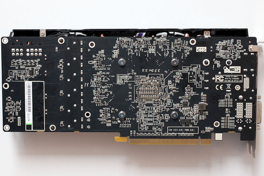
Pictured above are the front and back, showing the disassembled board. High-res versions are also available (front, back).
A Closer Look


Sapphire is using a vapor-chamber and four heatpipes to keep the card cool.
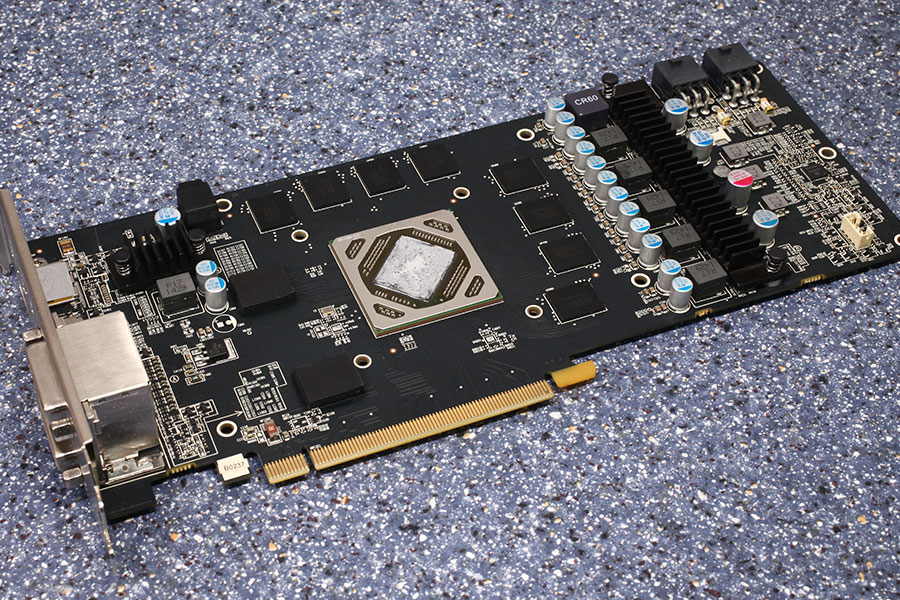
Two smaller heatsinks have been placed on the voltage-regulation circuitry. Near the GPU are two big black chunks that look a bit like memory chips. These are spacers to ensure the cooler doesn't wobble when installed.

Power delivery requires two 6-pin PCI-Express power connectors. This configuration is specified for up to 225 W power draw.

A BIOS switch is also available. It lets you switch between a legacy and UEFI BIOS and acts as a safeguard should something go wrong during a BIOS flash.

We've seen the NCP81022 voltage controller on Bonaire-based cards before. It is well supported in overclocking software and offers monitoring and voltage control.
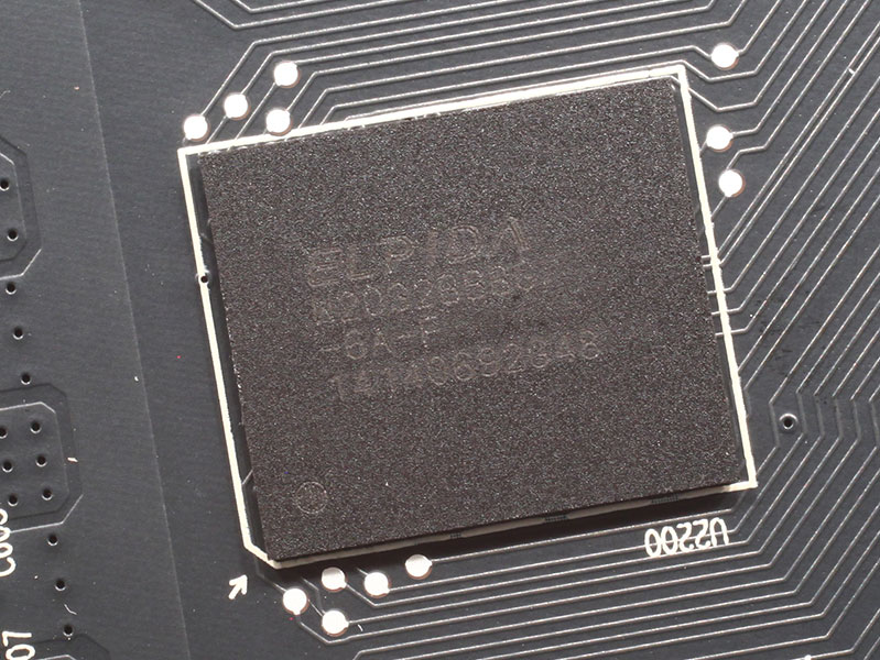
The GDDR5 memory chips are by Elpida and carry the model number W2032BBBG-6A-F. They are specified to run at 1500 MHz (6000 MHz GDDR5 effective).

AMD's Tonga graphics processor uses a new version of the GCN shader architecture. It is produced on a 28 nm process at TSMC, Taiwan, with a transistor count AMD does not provide. I measured its die size to be 17.5 x 20.9 mm = 366 mm², which makes the GPU bigger than Tahiti and, most probably, more expensive to produce.
Our Patreon Silver Supporters can read articles in single-page format.
May 6th, 2024 00:27 EDT
change timezone
Latest GPU Drivers
New Forum Posts
- Only some humans can see refresh rates faster than others, I am one of those humans. (142)
- Free Games Thread (3781)
- TPU's WCG/BOINC Team (34421)
- Apparently Valve is giving refunds on Helldivers 2 regardless of hour count. Details inside. (77)
- What software are you using to monitor CPU temps during gaming session? (21)
- Overheating/undervolt/setup issues (2)
- Alphacool CORE 1 CPU block - bulging with danger of splitting? (101)
- Current Sales, Bundles, Giveaways (10227)
- FINAL FANTASY XIV: Dawntrail Official Benchmark (84)
- The Official Thermal Interface Material thread (1157)
Popular Reviews
- Finalmouse UltralightX Review
- ASRock NUC BOX-155H (Intel Core Ultra 7 155H) Review
- Meze Audio LIRIC 2nd Generation Closed-Back Headphones Review
- Cougar Hotrod Royal Gaming Chair Review
- Upcoming Hardware Launches 2023 (Updated Feb 2024)
- Montech Sky Two GX Review
- AMD Ryzen 7 7800X3D Review - The Best Gaming CPU
- HYTE THICC Q60 240 mm AIO Review
- ASUS Radeon RX 7900 GRE TUF OC Review
- Logitech G Pro X Superlight 2 Review - Updated with 4000 Hz Tested
Controversial News Posts
- Intel Statement on Stability Issues: "Motherboard Makers to Blame" (240)
- Windows 11 Now Officially Adware as Microsoft Embeds Ads in the Start Menu (167)
- AMD to Redesign Ray Tracing Hardware on RDNA 4 (156)
- Sony PlayStation 5 Pro Specifications Confirmed, Console Arrives Before Holidays (117)
- AMD's RDNA 4 GPUs Could Stick with 18 Gbps GDDR6 Memory (114)
- NVIDIA Points Intel Raptor Lake CPU Users to Get Help from Intel Amid System Instability Issues (106)
- AMD Ryzen 9 7900X3D Now at a Mouth-watering $329 (104)
- AMD "Strix Halo" Zen 5 Mobile Processor Pictured: Chiplet-based, Uses 256-bit LPDDR5X (103)